
Bismuth Selenide Sputtering Target Description
A Bismuth Selenide Sputtering Target is a type of ceramic material composed of bismuth and selenium, commonly used in sputtering processes. This target is typically employed in thin film deposition and various specialized applications due to the unique properties of the bismuth-selenium combination.
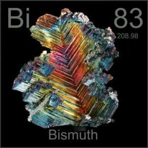 Bismuth is a chemical element with the symbol “Bi” and an atomic number of 83. The name “bismuth” originates from the German word ‘Bisemutum,’ a corruption of ‘Weisse Masse,’ meaning white mass. It was first used in 1753 and discovered by Claude François Geoffroy. Bismuth is located in Period 6 and Group 15 of the periodic table, belonging to the p-block elements. Its relative atomic mass is approximately 208.98040 Daltons, with the number in parentheses indicating a margin of uncertainty.
Related Product: Bismuth Sputtering Target
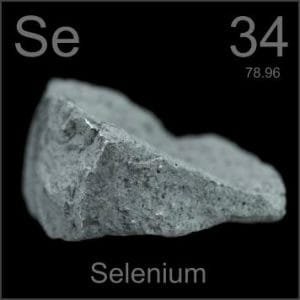 Selenium is a chemical element with the symbol “Se” and an atomic number of 34. The name “selenium” is derived from the Greek word ‘selene,’ meaning moon. It was first identified in 1817 by Jöns Jacob Berzelius and Johan Gottlieb Gahn, who also later accomplished and announced its isolation. Selenium is located in Period 4 and Group 16 of the periodic table, classified within the p-block elements. Its relative atomic mass is approximately 78.96 Daltons, with the number in parentheses indicating a margin of uncertainty.
Bismuth Selenide Sputtering Target Specification
| Compound Formula | Bi2Se3 |
| Appearance | Gray Solid |
| Density | 9.20 g/cm3 |
| Melting Point | 2,000 °C |
| Available Sizes | Dia.: 1.0″, 2.0″, 3.0″, 4.0″, 5.0″, 6.0″ Thick: 0.125″, 0.250″ |
Bismuth Selenide Sputtering Target Handing Notes
1. Indium bonding is recommended for Bismuth Selenide Sputtering Targets due to certain characteristics, such as brittleness and low thermal conductivity, which make them less amenable to sputtering.
2. Bismuth Selenide Sputtering Targets have low thermal conductivity and are susceptible to thermal shock.
Bismuth Selenide Sputtering Target Application
The Bismuth Selenide Sputtering Target is utilized in various applications, including thin film deposition and decorative coatings. It is commonly used in the semiconductor industry, display technologies, and the manufacturing of LEDs and photovoltaic devices. Additionally, this material plays a significant role in functional coatings, the optical information storage industry, glass coatings for automotive and architectural purposes, and optical communication technologies.
Bismuth Selenide Sputtering Target Packing
Our Bismuth Selenide Sputtering Targets are meticulously tagged and labeled on the exterior to ensure efficient identification and maintain high standards of quality control. We take extensive precautions to prevent any potential damage during storage and transportation, ensuring that the targets arrive in perfect condition.


Reviews
There are no reviews yet.