Bismuth Sputtering Target Description
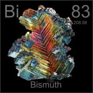 Bismuth sputtering targets share the same properties as metallic bismuth. Bismuth (Bi), with an atomic number of 83, is a chemical element named from the German ‘Bisemutum,’ derived from ‘Weisse Masse,’ meaning white mass. Located in Period 6, Group 15 of the periodic table, it is the most metallic and least abundant in the nitrogen group. Bismuth is hard, brittle, lustrous, and coarsely crystalline, distinguishable by its unique gray-white color with a reddish hue. Bismuth sputtering targets are widely used in aerospace, automotive lighting, OLED, and optical industries.
Bismuth Sputtering Target Specification
| Material Type | Bismuth |
| Symbol | Bi |
| Color/Appearance | Lustrous Reddish White, Metallic |
| Melting Point | 2079 °C |
| Boiling Point | 1560 °C |
| Density | 9.747 g/cm3 |
| Sputter | RF |
| Type of Bond | Indium, Elastomer |
| Comments | Resistivity high. Low Melting Point materials not ideal for sputtering. |
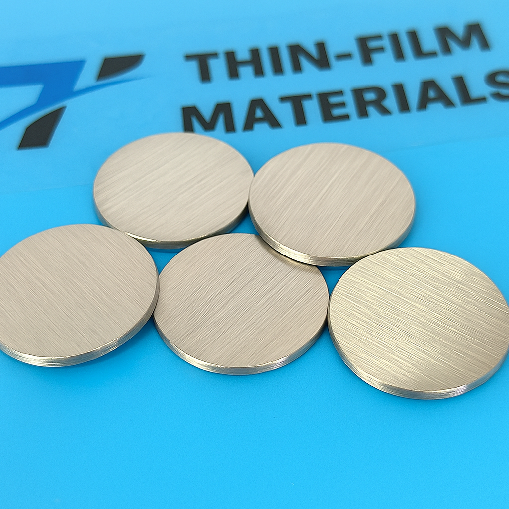
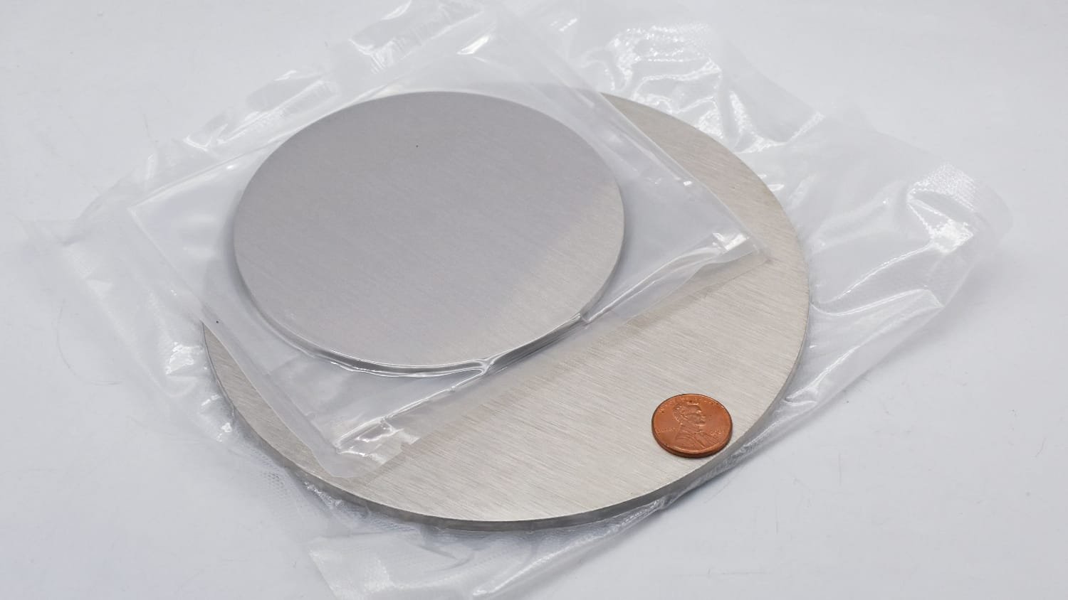
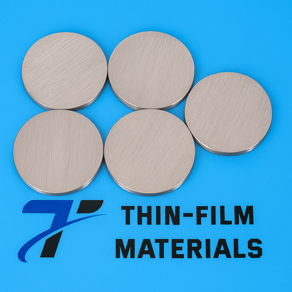
| Available Sizes | Dia.: 2.0″, 3.0″, 4.0″, 5.0″, 6.0″ Thick: 0.125″, 0.250″ |
We also offer other customized shapes and sizes of the sputtering targets; please Contact Us for more information.
Bismuth Sputtering Target Application
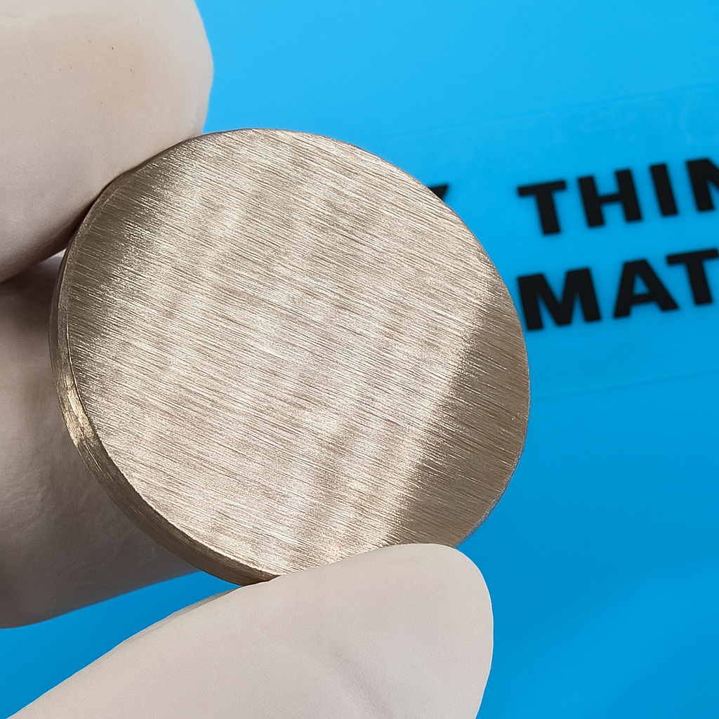
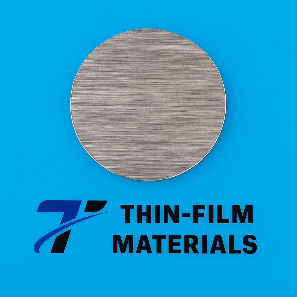
ø6″ Bismuth Targets made by Thin-Film Materials
Bismuth sputter targets are used for thin film deposition in applications such as fuel cells, decorative coatings, semiconductors, displays, LEDs, photovoltaic devices, and glass coatings. Other uses of bismuth include:
- Fusible alloys
- Cosmetics and pigments
- Low melting solders
- Pharmaceuticals
- Lead replacement
- Synthetic fibers
- Shot and shotgun pellets
Bismuth Sputtering Target Bonding Services
Specialized bonding services for Bismuth Sputtering Targets, including indium and elastomeric bonding techniques, enhance performance and durability. Thin Film Materials (TFM) ensures high-quality solutions that meet industry standards and customer needs.
We also offer custom machining of backing plates, which is essential for sputtering target assembly. This comprehensive approach improves target design flexibility and performance in thin film deposition. Our channels provide detailed information about bonding materials, methods, and services, helping clients make informed decisions.

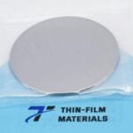
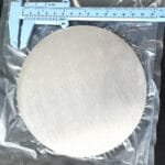
Bismuth Sputtering Target Packaging
Our Bismuth Sputtering Targets are clearly tagged and labeled externally to ensure efficient identification and quality control. We take great care to prevent any damage during storage and transportation.
Get Contact
TFM offers Bismuth Sputtering Targets in various forms, purities, sizes, and prices. We specialize in high-purity thin film deposition materials with optimal density and minimal grain sizes, which are ideal for semiconductor, CVD, and PVD applications in display and optics. Contact Us for current pricing on sputtering targets and other deposition materials that are not listed.


Reviews
There are no reviews yet.