
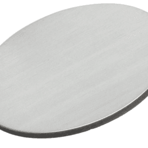
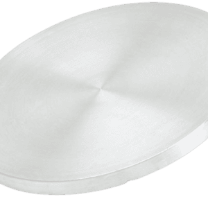
Bismuth Telluride Selenide N-Type Sputtering Target
Introduction
Bismuth Telluride Selenide N-Type Sputtering Target (commonly expressed as Bi₂Te₂.₇Se₀.₃) is an essential material for thermoelectric devices, semiconductor thin films, and advanced electronic components. Its finely tuned composition enables controlled carrier concentration and high Seebeck performance, making it indispensable for research laboratories and microelectronics manufacturers working on next-generation thermal-management technologies.
Detailed Description
The Bismuth Telluride Selenide N-Type Sputtering Target is engineered with a carefully optimized Bi–Te–Se ratio to balance electrical conductivity, thermal conductivity, and stability during sputtering.
N-type thermoelectric characteristics: Selenium substitution introduces additional free electrons, enhancing electrical transport properties required for high-performance thermoelectric thin films.
Dense microstructure: Manufactured by vacuum hot pressing or cold isostatic pressing followed by sintering to achieve high density and uniform grain distribution, essential for consistent sputtering rates.
Stable sputtering behavior: The composition minimizes volatilization of Te during deposition and improves film uniformity for semiconductor-grade thermoelectric layers.
High purity: Typical purities range from 99.9% to 99.999%, supporting clean, defect-free film growth for precision device applications.
These characteristics make the target particularly suitable for thermoelectric thin-film development, micro-cooling modules, and material optimization studies.
Applications
Thermoelectric devices (Peltier coolers, micro-coolers, energy harvesting modules)
Semiconductor thermal management thin films
Thermoelectric sensors and IR detectors
Research on N-type Bi–Te–Se alloy systems
Thin-film thermoelectric generators
MEMS and microelectronics requiring localized cooling
Technical Parameters
| Parameter | Typical Value / Range | Importance |
|---|---|---|
| Purity | 99.9% – 99.999% | Higher purity improves electrical properties and film reproducibility |
| Composition | Bi₂Te₂.₇Se₀.₃ (N-type) | Provides optimized carrier concentration |
| Diameter | 25 – 300 mm (custom) | Compatible with standard sputtering systems |
| Thickness | 3 – 6 mm | Influences sputtering stability and target lifetime |
| Density | ≥ 95% theoretical | Ensures uniform erosion and film consistency |
| Bonding | Indium / Elastomer / Copper backing | Enhances thermal conductivity and prevents cracking |
Comparison with Related Materials
| Material | Key Advantage | Typical Application |
|---|---|---|
| Bi₂Te₂.₇Se₀.₃ (N-type) | High Seebeck coefficient and optimized electron concentration | Thermoelectric cooling thin films |
| Bi₀.₅Sb₁.₅Te₃ (P-type) | High performance for complementary P-leg | Complete thermoelectric modules |
| Bi₂Te₃ | Lower cost & widely used baseline TE material | General thermoelectric R&D |
FAQ
| Question | Answer |
|---|---|
| Can the target be customized? | Yes. Purity, diameter, thickness, and bonding can be tailored to your deposition system. |
| What is the packaging method? | Vacuum-sealed, anti-shock foam protected, shipped in export-grade cartons or wooden crates. |
| Is bonding necessary? | Recommended for large-diameter targets to improve heat dissipation and prevent cracking. |
| What deposition systems are compatible? | DC/RF magnetron sputtering systems used in semiconductor and thermoelectric research. |
| Does the element ratio affect film properties? | Yes, the Bi–Te–Se ratio directly determines carrier type, concentration, and thermoelectric efficiency. |
Packaging
Each Bismuth Telluride Selenide N-Type Sputtering Target is vacuum-sealed and externally labeled for traceability. Additional cushioning and rigid outer packaging ensure safe transport and prevent chipping or oxidation during storage.
Conclusion
The Bismuth Telluride Selenide N-Type Sputtering Target offers a precise balance of electrical efficiency, stability, and reproducibility for thermoelectric thin-film development. With customizable dimensions, bonding options, and high purity grades, it provides a reliable solution for advanced research and industrial sputtering applications.
For detailed specifications or a quotation, please contact us at sales@thinfilmmaterials.com

Reviews
There are no reviews yet.