
Boron Carbide Sputtering Target
Introduction
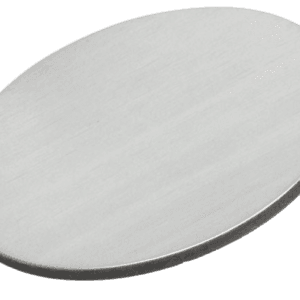
Boron Carbide (B₄C) Sputtering Target is a highly durable ceramic material widely used in thin film deposition processes. Known for its exceptional hardness, chemical stability, and resistance to high temperatures, B₄C targets are essential in applications where wear resistance, protective coatings, and advanced semiconductor properties are required. Their ability to form uniform and adherent films makes them an indispensable material in modern industries.
Detailed Description
Boron Carbide is one of the hardest known materials, ranking just below diamond and cubic boron nitride. As a sputtering target, B₄C offers:
Exceptional hardness and wear resistance – ensuring long service life in demanding deposition processes.
High thermal stability – suitable for high-temperature environments.
Low density compared to other ceramics – making it advantageous where lightweight films are needed.
Chemical inertness – providing resistance to corrosion, oxidation, and acidic environments.
These features make Boron Carbide films particularly valuable for coatings that need to withstand mechanical stress and corrosive conditions.
Applications
Boron Carbide Sputtering Targets are used across a wide range of industries, including:
Semiconductors – thin films for electronic devices.
Hard protective coatings – tools, dies, and wear components.
Optical coatings – scratch-resistant and durable thin films.
Nuclear industry – neutron absorption layers due to boron’s high neutron cross-section.
Defense and aerospace – lightweight, impact-resistant coatings.
Technical Parameters
| Parameter | Typical Value / Range | Importance |
|---|---|---|
| Purity | 99% – 99.9% | Higher purity ensures improved film performance |
| Diameter | 25 – 300 mm (custom sizes) | Fits a variety of sputtering systems |
| Thickness | 3 – 10 mm | Influences deposition rate and uniformity |
| Density | ≥ 95% of theoretical | Ensures stable sputtering behavior |
| Bonding | Indium / Elastomer / Copper | Enhances thermal conductivity and mechanical stability |
Comparison with Related Materials
| Material | Key Advantage | Typical Application |
|---|---|---|
| Boron Carbide (B₄C) | Extreme hardness, neutron absorption | Wear-resistant & nuclear coatings |
| Titanium Nitride (TiN) | High adhesion and conductivity | Decorative & cutting tool coatings |
| Silicon Carbide (SiC) | Thermal stability, chemical resistance | Electronics, aerospace components |
FAQ
| Question | Answer |
|---|---|
| Can the Boron Carbide Sputtering Target be customized? | Yes, we can adjust purity, size, thickness, and backing options to your requirements. |
| What is the typical lead time? | Generally 2–3 weeks, depending on order size and specifications. |
| How are the targets packaged? | Vacuum-sealed with protective foam, packed in export-safe cartons or wooden crates. |
| Which industries use Boron Carbide targets the most? | Semiconductor, defense, optics, aerospace, and energy research. |
Packaging
Our Boron Carbide Sputtering Targets are carefully vacuum-sealed and externally labeled for clear identification. Each target is cushioned with protective materials and placed in sturdy export-grade cartons or wooden crates to ensure safe delivery and prevent damage during transportation.
Conclusion
Boron Carbide Sputtering Targets combine extreme hardness, chemical stability, and unique physical properties that make them essential for advanced thin film deposition. With customizable sizes, bonding options, and high-purity grades, they are widely adopted in semiconductor, aerospace, defense, and optical industries.
For detailed specifications and a quotation, please contact us at sales@thinfilmmaterials.com.


Reviews
There are no reviews yet.