Generic selectors
Exact matches only
Search in title
Search in content
Post Type Selectors

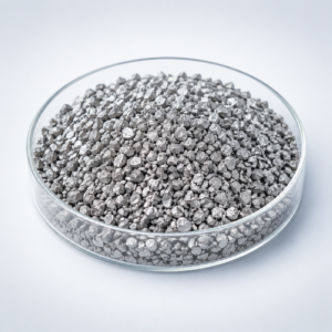
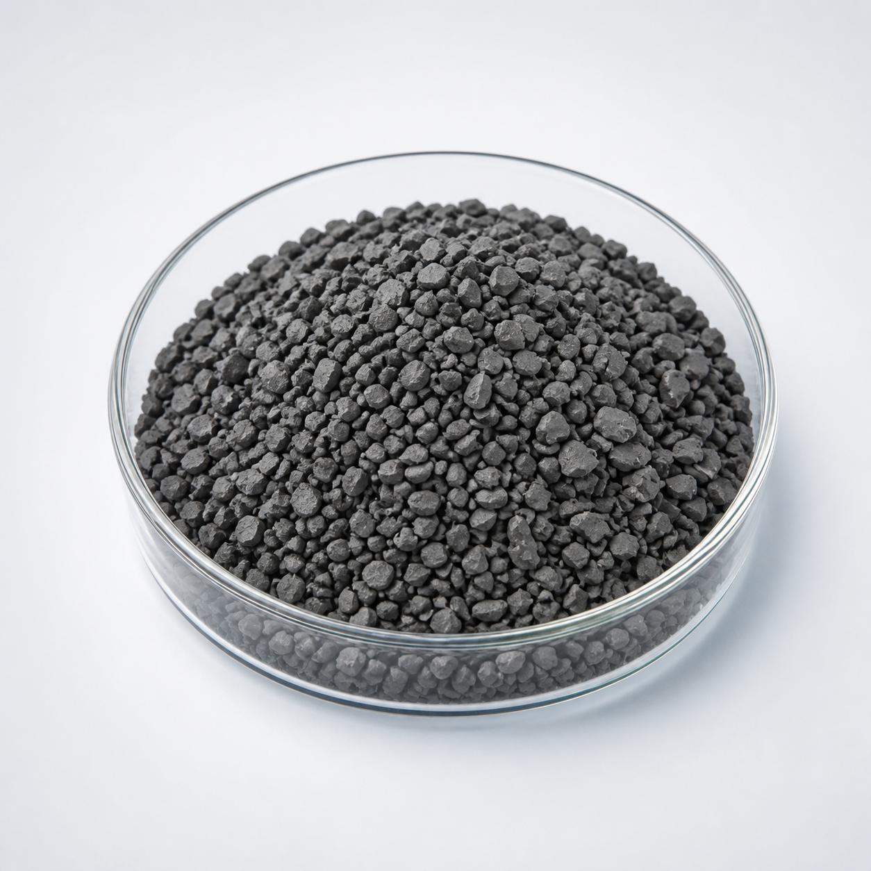
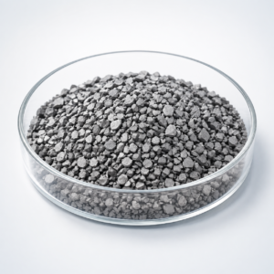
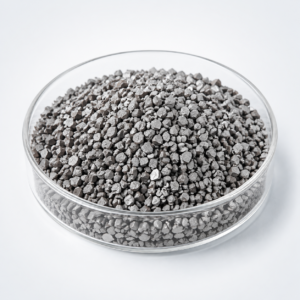
Boron (B) Evaporation Materials

Material: Boron
Chemical Formula: B
Catalog No.: TFM-EVM-0042
Purity: 99.5%
Color/Appearance: Black, Semi-metallic
Shape: Powder/ Granule/ Custom-made

Boron evaporation material is supplied by Thin Film Materials (TFM) for vacuum evaporation and thin-film deposition. Available form, size, purity, and packaging can be customized to suit research and production requirements.

Product Overview

Boron (B) Evaporation Materials (B) is an elemental evaporation source for optical, electronic, semiconductor, and compound-film development. These materials can differ substantially in vapor pressure, reactivity, and thermal behavior, so evaporation method and source hardware should be selected from the actual material properties rather than by product name alone. Clean handling and controlled preconditioning are especially useful when film composition or contamination limits are tight.


boron evaporation materials

Evaporation Behavior and Process Considerations

Source heating should be matched to the material’s vapor-pressure curve and reactivity. Some materials sublime or evaporate before forming a conventional melt, while others require localized e-beam heating. A controlled ramp, clean source hardware, and rate monitoring can reduce sudden outgassing or unstable flux.

Technical Data

Material TypeBoron
SymbolB
Color/AppearanceBlack, Semi-metallic
Melting Point271.3 °C
Boiling Point2550 °C
Density2.34 cryst. g/cm3
Thermal Conductivity27 W/m.K

Typical Thin-Film Applications

  • Thin-film R&D requiring a composition-specific evaporation source
  • Optical, semiconductor, electronic, energy, and advanced-material coating studies depending on the compound
  • Custom PVD research using pellets, pieces, granules, or other source forms

Source Form and Ordering Considerations

For quotation, provide material, purity, source form, particle or piece size, quantity, evaporation method, and any boat, basket, crucible, or e-beam hearth constraints. If the material will be used for a specific coating stack, sharing the intended film thickness or deposition application can help with source-form selection and packaging recommendations.

Frequently Asked Questions

How should the evaporation method for Boron (B) be selected?

Select the method from melting point, vapor pressure, decomposition behavior, charge size, and the available source hardware. Resistance heating and electron-beam evaporation are the most common starting options.

What source form is available for Boron (B)?

Depending on the material, pellets, pieces, granules, tablets, or other compact forms can be reviewed for compatibility with the customer’s evaporator.

Why is source preconditioning important for Boron (B)?

Gradual preheating can remove adsorbed gas, stabilize the charge, and reduce spitting or pressure excursions before film deposition.

Can the film composition differ from the Boron (B) source?

Yes. Preferential evaporation, decomposition, re-evaporation, and substrate conditions can all change the final film composition.

Does purity matter for Boron (B) evaporation material?

Yes. Source purity contributes directly to the contamination budget of the deposited film, together with chamber, crucible, and substrate cleanliness.

What information should I send TFM for a Boron (B) RFQ?

Provide material or formula, purity, source form and size, quantity, evaporation method, holder constraints, and any film or documentation requirements.
Reviews

There are no reviews yet.

Be the first to review “Boron (B) Evaporation Materials”

Your email address will not be published. Required fields are marked *

FAQ

  • They are high‐purity substances (e.g. metals, alloys, or compounds) used in thermal or electron‐beam evaporation processes to form thin films on substrates.

  • Typically, they’re processed into a form (often ingots, pellets, or wires) that can be efficiently vaporized. Preparation emphasizes high purity and controlled composition to ensure film quality.

  • Thermal evaporation and electron-beam (e-beam) evaporation are the two main techniques, where material is heated (or bombarded with electrons) until it vaporizes and then condenses on the substrate.

  • Thermal evaporation heats the material directly (often using a resistive heater), while e-beam evaporation uses a focused electron beam to locally heat and vaporize the source material—each method offering different control and energy efficiency.

  • Key parameters include source temperature, vacuum level, deposition rate, substrate temperature, and the distance between the source and the substrate. These factors influence film uniformity, adhesion, and microstructure.

  • Evaporation generally produces high-purity films with excellent control over thickness, and it is especially suitable for materials with relatively low melting points or high vapor pressures.

  • Challenges include issues with step coverage (due to line-of-sight deposition), shadowing effects on complex topographies, and possible re-evaporation of material from the substrate if temperature isn’t properly controlled.

  • Common evaporation materials include noble metals (e.g., gold, silver), semiconductors (e.g., silicon, germanium), metal oxides, and organic compounds—each chosen for its specific optical, electrical, or mechanical properties.

  • Selection depends on desired film properties (conductivity, optical transparency, adhesion), compatibility with the evaporation process, and the final device application (semiconductor, optical coating, etc.).

  • Optimizing substrate temperature, deposition rate, and chamber vacuum are critical for ensuring that the film adheres well and forms the intended microstructure without defects.

  • Troubleshooting may involve checking the source material’s purity, ensuring stable source temperature, verifying the vacuum level, adjusting the substrate’s position or temperature, and monitoring deposition rate fluctuations.

While evaporation tends to yield very high purity films with excellent thickness control, it is limited by its line-of-sight nature. In contrast, sputtering can deposit films more uniformly on complex surfaces and is more versatile for a broader range of materials.


Shopping Cart
Scroll to Top