Boron Nitride Sputtering Target Description
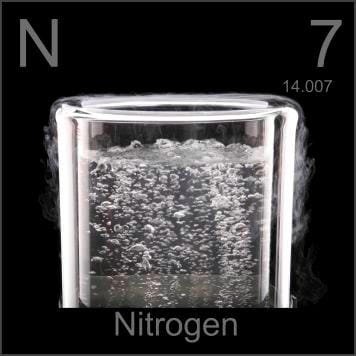
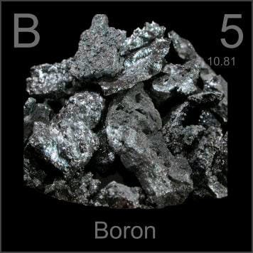 Boron nitride sputtering targets, containing the elements boron (B) and nitrogen (N), are provided by TFM. Boron nitride (BN) is a ceramic material known for its high heat capacity, excellent thermal conductivity, low dielectric constant, and superior dielectric strength. These properties make BN an outstanding material for various applications. Additionally, boron nitride is easy to process and has non-adhesive qualities, enhancing its versatility and usability in different industries.
Related Product: Boron Sputtering Target
Boron Nitride Sputtering Target Specification
| Material Type | Boron Nitride |
| Symbol | BN |
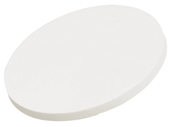
| Color/Appearance | White, Crystalline Solid |
| Melting Point | ~3,000 °C |
| Theoretical Density | 2.25 g/cc |
| Sputter | RF, RF-R |
| Type of Bond | Indium, Elastomer |
| Comments | Decomposes when sputtered. Reactive preferred. |
| Available Sizes | Dia.: 1.0″, 2.0″, 3.0″, 4.0″, 5.0″, 6.0″ Thick: 0.125″, 0.250″ |
We also offer other customized shapes and sizes of the sputtering targets; please Contact Us for more information.
Boron Nitride Sputtering Target Applications
Boron nitride sputtering targets are widely used for thin film deposition in applications such as fuel cells, decorative coatings, electrical insulation, semiconductors, displays, LEDs, and photovoltaic devices, as well as glass coating. The excellent thermal and chemical stability of boron nitride ceramics makes them suitable for high-temperature equipment components. In the field of nanotechnology, BN nanotubes, which have a similar structure to carbon nanotubes but with different properties, show great potential. Hexagonal boron nitride (h-BN) ceramics are often used to manufacture BN crucibles. Cubic boron nitride (c-BN) serves as an abrasive material and is ideal for heat spreaders. Additionally, amorphous boron nitride (a-BN) layers are utilized in various semiconductor devices.
Target Bonding of Boron Nitride Sputtering Target
Specialized bonding services for Boron Nitride Sputtering Targets, including indium and elastomeric bonding techniques, enhance performance and durability. Thin Film Materials (TFM) ensures high-quality solutions that meet industry standards and customer needs.
We also offer custom machining of backing plates, which is essential for sputtering target assembly. This comprehensive approach improves target design flexibility and performance in thin film deposition. Our channels provide detailed information about bonding materials, methods, and services, helping clients make informed decisions.

Packaging
Our boron nitride sputter targets are meticulously tagged and labeled externally to ensure clear identification and stringent quality control. We take special precautions in handling and packaging to prevent any damage during storage or transportation, ensuring that our products arrive in optimal condition.


Reviews
There are no reviews yet.