Introduction
Boron Sputtering Targets (B) are essential materials in advanced thin film deposition processes where extreme hardness, thermal stability, and precise chemical control are required. As a lightweight metalloid with unique bonding characteristics, boron is widely used in semiconductor manufacturing, protective coatings, neutron detection, and research-driven thin film applications. Boron sputtering targets enable the direct deposition of boron-containing films with excellent uniformity and reproducibility.
Detailed Description
Boron sputtering targets are typically produced from high-purity boron powder through hot pressing or sintering under controlled conditions. Due to boron’s intrinsic hardness and brittleness, manufacturing requires precise control of particle size, temperature, and pressure to achieve sufficient density and mechanical integrity for stable sputtering performance.
Compared with metallic targets, elemental boron exhibits low electrical conductivity, which makes RF sputtering the preferred deposition method in most applications. Boron targets demonstrate consistent erosion behavior and allow accurate control over film composition, especially in applications where stoichiometry and impurity levels are critical.
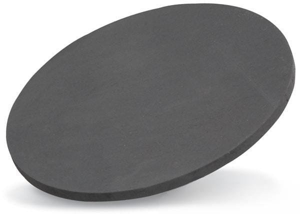
High-purity boron targets help minimize contamination from oxygen, carbon, or metallic impurities, directly impacting film performance in semiconductor and optical systems. Targets can be supplied as monolithic discs or plates, or bonded to metallic backing plates (such as copper) to improve heat dissipation and reduce the risk of cracking during operation.
Applications
Boron Sputtering Targets are widely used in:
Semiconductor and microelectronics manufacturing
Boron-doped thin films for electronic devices
Hard and wear-resistant coatings
Neutron detection and nuclear research coatings
Diffusion barriers and passivation layers
Advanced research and development applications
Technical Parameters
| Parameter | Typical Value / Range | Importance |
|---|---|---|
| Chemical Symbol | B | Defines elemental boron films |
| Purity | 99.5% – 99.99% | Reduces contamination and defects |
| Crystal Form | Amorphous / Polycrystalline | Influences sputtering behavior |
| Diameter | 25 – 300 mm (custom) | Matches sputtering cathodes |
| Thickness | 3 – 6 mm (typical) | Affects target lifetime |
| Sputtering Mode | RF (preferred) | Required due to low conductivity |
| Backing Plate | Copper (optional) | Enhances thermal stability |
Comparison with Related Boron-Based Targets
| Material | Key Advantage | Typical Application |
|---|---|---|
| Boron (B) | Pure boron films | Semiconductor & research |
| Boron Carbide (B₄C) | Extreme hardness | Protective coatings |
| Boron Nitride (BN) | Electrical insulation | Dielectric thin films |
FAQ
| Question | Answer |
|---|---|
| Why is RF sputtering required for boron targets? | Elemental boron has low electrical conductivity, making RF sputtering more stable. |
| Can boron targets be bonded to backing plates? | Yes, bonding to copper backing plates is available. |
| Are custom sizes supported? | Yes, diameter, thickness, and shape can be customized. |
| Is boron suitable for reactive sputtering? | Yes, boron can be used in reactive processes depending on film requirements. |
| How is the target packaged? | Vacuum-sealed with moisture protection and impact-resistant packaging. |
Packaging
Our Boron Sputtering Targets are carefully cleaned, vacuum-sealed, and packaged using moisture-resistant materials to prevent oxidation and contamination. Each target is clearly labeled to ensure traceability and consistent quality control throughout storage and transportation.
Conclusion
Boron Sputtering Target (B) is a high-performance material for producing boron-based thin films with exceptional purity and stability. With customizable dimensions, high-density fabrication, and optional backing plates, boron targets provide reliable performance for semiconductor, protective coating, and advanced research applications.
For detailed specifications and a quotation, please contact us at sales@thinfilmmaterials.com.


Reviews
There are no reviews yet.