
 MSDS File
| Material Type | Cadmium Antimony |
| Symbol | CdSb |
| Melting Point (°C) | |
| Theoretical Density (g/cc) |
| Z Ratio | |
| E-Beam | |
| E-Beam Crucible Liner Material | |
| Temp. (°C) for Given Vap. Press. (Torr) | |
| Comments |
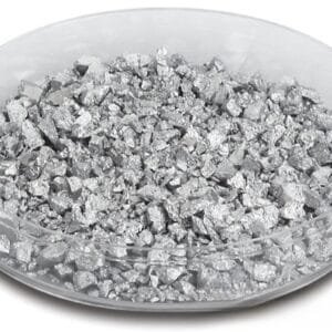
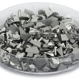
Cadmium Antimony Pellet Evaporation Material
TFM provides high-purity Cadmium Antimony Pellet Evaporation Material, a valuable compound for thin-film deposition, optoelectronics, and semiconductor applications. Known for its outstanding optical and electrical properties, this material is extensively used in photovoltaic cells, infrared sensors, and advanced electronic devices.
Key Features and Advantages
High Purity (99.99% – 99.999%) – Guarantees optimal performance in thin-film deposition and electronic applications.
Excellent Optical & Electrical Properties – Ensures high absorption efficiency for solar cells and optoelectronic devices.
Optimized for Thin-Film Deposition – Compatible with thermal evaporation and E-beam evaporation processes.
Stable & Uniform Coating – Delivers consistent film quality, which is critical for high-efficiency devices.
Customizable Composition – The Cd/Sb ratio can be adjusted to meet specific application requirements.
Applications
Thin-Film Solar Cells – Ideal for enhancing solar energy conversion in photovoltaic technologies.
Optoelectronic Devices – Used in infrared detectors, photodetectors, and LEDs.
Semiconductor Research & Development – Supports cutting-edge material science in the electronics industry.
Thin-Film Transistors & Sensors – Applied in wearable electronics, transparent electronics, and smart devices.
Industry Impact
TFM’s Cadmium Antimony Pellet Evaporation Material is a high-performance material that plays a key role in advancements in solar energy, optoelectronics, and semiconductor technologies. Its high purity, superior light absorption, and optimized deposition characteristics ensure high-quality films, making it an ideal choice for renewable energy applications and innovative electronic device fabrication.

Reviews
There are no reviews yet.