Generic selectors
Exact matches only
Search in title
Search in content
Post Type Selectors

VD0842 Cadmium Selenide Evaporation Materials, CdSe

Catalog No.VD0842
MaterialCadmium Selenide (CdSe)
Purity99.9% ~ 99.999%
ShapePowder/ Granule/ Custom-made

TFM stands as a premier provider of top-grade cadmium selenide evaporation materials, along with an extensive range of other evaporation materials. Our offerings include both powder and granule forms, with custom formats available to meet specific requirements upon request.

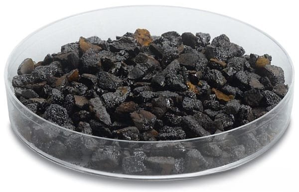
Cadmium Selenide Evaporation Materials Overview

TFM offers high-quality cadmium selenide evaporation materials, known for their exceptional performance in thin-film deposition applications. With the chemical formula CdSe, this selenide ceramic evaporation material is available in high-purity grades, up to 99.9995%, ensuring the production of high-quality deposited films. TFM employs strict quality control measures, making their CdSe materials reliable for critical industrial processes.

Related Products: Cadmium Evaporation Materials

Specifications of Cadmium Selenide Evaporation Materials

Material TypeCadmium selenide
SymbolCdSe
Appearance/ColorBlack crystal
Melting Point710 °C (1,310 °F; 983 K)
Density6.82 g/cm3
Purity99.9% ~ 99.999%
ShapePowder/ Granule/ Custom-made

Applications of Cadmium Selenide Evaporation Materials

Cadmium selenide evaporation materials are primarily used in various deposition processes such as semiconductor deposition, chemical vapor deposition (CVD), and physical vapor deposition (PVD). These materials are essential in optical applications, including wear-resistant coatings, decorative finishes, and display technologies.

Packaging and Handling of Cadmium Selenide Evaporation Materials

To ensure easy identification and maintain product integrity, TFM carefully labels and packages cadmium selenide evaporation materials. Special attention is given to prevent damage during both storage and transportation, ensuring the materials reach customers in excellent condition.

Contact TFM for Custom Solutions

As a leading supplier of high-purity cadmium selenide evaporation materials, TFM offers a variety of shapes such as tablets, granules, rods, and wires. Custom sizes and quantities are available upon request. In addition, TFM provides a comprehensive range of evaporation accessories including boats, filaments, crucibles, heaters, and e-beam crucible liners. Feel free to reach out for pricing details and further inquiries regarding additional products not listed.

Reviews

There are no reviews yet.

Be the first to review “VD0842 Cadmium Selenide Evaporation Materials, CdSe”

Your email address will not be published. Required fields are marked *

FAQ

  • They are high‐purity substances (e.g. metals, alloys, or compounds) used in thermal or electron‐beam evaporation processes to form thin films on substrates.

  • Typically, they’re processed into a form (often ingots, pellets, or wires) that can be efficiently vaporized. Preparation emphasizes high purity and controlled composition to ensure film quality.

  • Thermal evaporation and electron-beam (e-beam) evaporation are the two main techniques, where material is heated (or bombarded with electrons) until it vaporizes and then condenses on the substrate.

  • Thermal evaporation heats the material directly (often using a resistive heater), while e-beam evaporation uses a focused electron beam to locally heat and vaporize the source material—each method offering different control and energy efficiency.

  • Key parameters include source temperature, vacuum level, deposition rate, substrate temperature, and the distance between the source and the substrate. These factors influence film uniformity, adhesion, and microstructure.

  • Evaporation generally produces high-purity films with excellent control over thickness, and it is especially suitable for materials with relatively low melting points or high vapor pressures.

  • Challenges include issues with step coverage (due to line-of-sight deposition), shadowing effects on complex topographies, and possible re-evaporation of material from the substrate if temperature isn’t properly controlled.

  • Common evaporation materials include noble metals (e.g., gold, silver), semiconductors (e.g., silicon, germanium), metal oxides, and organic compounds—each chosen for its specific optical, electrical, or mechanical properties.

  • Selection depends on desired film properties (conductivity, optical transparency, adhesion), compatibility with the evaporation process, and the final device application (semiconductor, optical coating, etc.).

  • Optimizing substrate temperature, deposition rate, and chamber vacuum are critical for ensuring that the film adheres well and forms the intended microstructure without defects.

  • Troubleshooting may involve checking the source material’s purity, ensuring stable source temperature, verifying the vacuum level, adjusting the substrate’s position or temperature, and monitoring deposition rate fluctuations.

While evaporation tends to yield very high purity films with excellent thickness control, it is limited by its line-of-sight nature. In contrast, sputtering can deposit films more uniformly on complex surfaces and is more versatile for a broader range of materials.


Shopping Cart
Scroll to Top