Introduction
Cadmium Selenide (CdSe) sputtering targets are widely used for depositing II–VI semiconductor thin films with well-defined optical and electronic properties. Known for its direct bandgap and strong light absorption in the visible spectrum, CdSe is a key material in optoelectronic devices, photovoltaics, and quantum dot technologies. High-quality CdSe sputtering targets enable precise control over film composition and are essential for achieving reproducible device performance.
Detailed Description
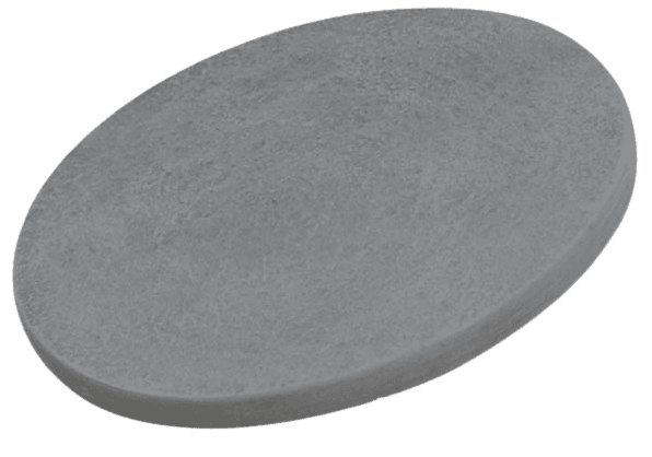
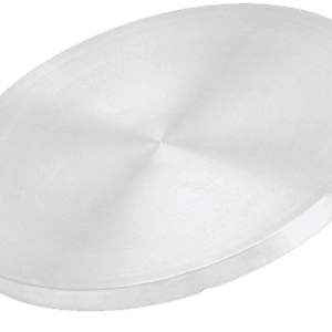
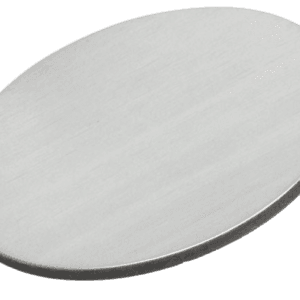
CdSe sputtering targets are manufactured with strict control over stoichiometry (Cd:Se ≈ 1:1) and microstructure to ensure stable sputtering behavior and uniform film deposition. Production methods such as vacuum hot pressing or sintering are commonly used to achieve high density and minimize porosity, which is critical for reducing particle generation and ensuring consistent erosion during sputtering.
Cadmium Selenide exhibits a direct bandgap of approximately 1.74 eV at room temperature, making it highly suitable for light-emitting and light-absorbing applications. The material supports efficient electron-hole pair generation, which is beneficial for photodetectors, solar cells, and LEDs.
Due to the volatility of selenium and the toxicity of cadmium, careful handling and processing are required during both target fabrication and sputtering. High-density targets help maintain compositional uniformity and reduce preferential sputtering effects. For improved thermal management and mechanical stability, CdSe targets are often bonded to copper backing plates.
Key features include:
Controlled stoichiometry for consistent semiconductor properties
High density and low porosity for stable sputtering performance
Strong optical absorption and direct bandgap behavior
Suitable for RF magnetron sputtering of compound semiconductors
Customizable dimensions, purity levels, and bonding configurations
Applications
Cadmium Selenide sputtering targets are widely used in:
Thin film solar cells and photovoltaic research
Photodetectors and optical sensors
Light-emitting devices (LEDs) and display technologies
Quantum dot materials and nanostructures
Thin film transistors and semiconductor devices
Research in optoelectronics and nanotechnology
Technical Parameters
| Parameter | Typical Value / Range | Importance |
|---|---|---|
| Composition | CdSe (Cd:Se ≈ 1:1) | Determines optical and electronic properties |
| Purity | 99.9% – 99.99% | Reduces defect levels in films |
| Density | ≥ 95% – 99% theoretical | Ensures stable sputtering behavior |
| Diameter | 25 – 200 mm (custom) | Compatible with sputtering systems |
| Thickness | 3 – 6 mm | Affects target lifetime |
| Bonding | Copper backing (In / elastomer) | Improves heat dissipation |
| Sputtering Method | RF magnetron | Preferred for compound materials |
Comparison with Related Materials
| Material | Key Advantage | Typical Application |
|---|---|---|
| CdSe | Direct bandgap, strong visible absorption | Optoelectronics, quantum dots |
| CdTe | High photovoltaic efficiency | Solar cells |
| ZnSe | Wide bandgap, optical transparency | Optical coatings |
| PbSe | Infrared sensitivity | IR detectors |
FAQ
| Question | Answer |
|---|---|
| Can the CdSe target be customized? | Yes, dimensions, purity, and bonding options can be tailored to specific needs. |
| What sputtering method is recommended? | RF magnetron sputtering is typically used for CdSe deposition. |
| Are there safety considerations? | Yes, cadmium compounds are toxic; proper handling and ventilation are required. |
| Is stoichiometry critical? | Yes, maintaining the Cd:Se ratio is essential for consistent film performance. |
| What industries use CdSe most? | Photovoltaics, optoelectronics, and nanotechnology research. |
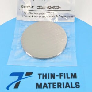
Packaging
Our Cadmium Selenide Sputtering Targets are meticulously tagged and labeled externally to ensure efficient identification and maintain high standards of quality control. We take great care to prevent any potential damage during storage and transportation, ensuring the targets arrive in perfect condition.
Conclusion
Cadmium Selenide sputtering targets provide a reliable solution for producing high-quality semiconductor thin films with excellent optical and electronic performance. With precise composition control and customizable configurations, they are ideal for advanced optoelectronic devices, photovoltaic systems, and cutting-edge research.
For detailed specifications and a quotation, please contact us at sales@thinfilmmaterials.com.
Reviews
There are no reviews yet.