
Product Overview
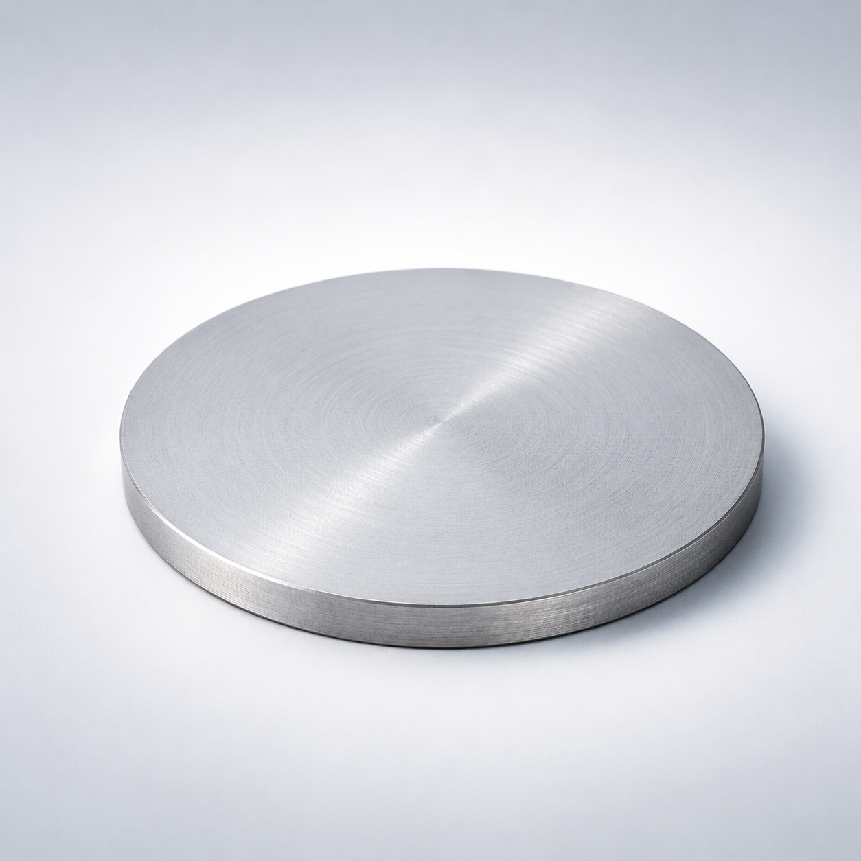
Cadmium Sputtering Target (Cd) is a conductive sputtering target used to deposit elemental thin films where purity, film cleanliness, and stable metallic sputtering behavior are important. For thin-film applications, the practical selection criteria are not limited to the target chemistry alone: purity grade, target density, dimensions, grain structure, surface finish, and backing configuration can all influence process stability and film quality.
Material and Deposition Characteristics
Because the target is electrically conductive, DC magnetron sputtering is often applicable, although pulsed-DC or other power modes may also be used depending on the deposition system and film target. For high-specification films, target grain structure, residual stress, and surface preparation can influence erosion uniformity and the morphology of the deposited layer. When higher power loading or system-specific mounting is involved, a bonded target assembly may also be considered.
Technical Data
| Parameter | Typical Value / Range | Importance |
|---|---|---|
| Chemical Symbol | Cd | Defines elemental sputtering material |
| Purity | 99.9% – 99.999% | Higher purity improves semiconductor performance |
| Diameter | 25 – 300 mm (custom) | Matches sputtering cathode holders |
| Thickness | 3 – 10 mm | Influences target lifetime |
| Density | ~8.65 g/cm³ | Relevant for deposition rate calculation |
| Bonding | Copper backing recommended | Enhances heat dissipation & stability |
| Material | Key Advantage | Typical Application |
|---|---|---|
| Cadmium (Cd) | Key II–VI semiconductor element | CdTe & CdS thin films |
| Zinc (Zn) | Lower toxicity alternative | ZnO & compound semiconductors |
| Tellurium (Te) | Compound formation with Cd | CdTe photovoltaics |
| Sulfur (S) | Forms CdS | Buffer layers in solar cells |
| Question | Answer |
|---|---|
| Is copper backing required? | It is strongly recommended for improved thermal management. |
| Is Cd compatible with DC sputtering? | Yes, cadmium’s conductivity allows for DC magnetron sputtering. |
| Can ultra-high purity grades be supplied? | Yes, up to 5N purity is available for semiconductor applications. |
| Are there handling considerations? | Yes, cadmium requires proper industrial handling due to toxicity regulations. |
| Is customization available? | Yes, size, thickness, and bonding configurations can be tailored. |
Typical Thin-Film Applications
- Cadmium thin films for conductive, optical, catalytic, or functional coating development
- Semiconductor, energy, electronic, or laboratory PVD research depending on the element
- Projects requiring a pure elemental source in planar or custom target geometry
Target Configuration and Ordering Considerations
For quotation and manufacturability review, provide target size, thickness, purity or alloy composition, quantity, and the sputtering gun or cathode model if known. If a bonded assembly is required, include backing-plate material, bonding preference, and any dimensional tolerances, surface-finish needs, or inspection-document requirements. TFM can also review customer drawings or old-target samples for replacement builds.
Frequently Asked Questions
Can Cadmium sputtering targets be used with DC magnetron sputtering?
Yes. Conductive metallic targets are commonly processed with DC magnetron sputtering, although pulsed-DC or other modes may also be used depending on the equipment and film objective.
What purity grade should I choose for a Cadmium target?
The required purity should be selected from the contamination limits and performance needs of the deposited film. Higher purity can reduce unwanted impurities, but the optimum grade should match the application rather than default to the highest available level.
Why do density and microstructure matter for Cadmium targets?
Target density, grain structure, and residual stress can influence erosion behavior, process stability, and the morphology of the deposited film. These factors become more important as film-quality requirements become tighter.
Can a Cadmium target be bonded to a copper backing plate?
Yes. A bonded assembly may be used when the cathode design requires a backing plate or when improved support and heat transfer are desirable. The bonding method should be matched to target thickness and operating conditions.
What are common applications of sputtered Cadmium films?
Typical uses include conductive layers, metallization, reflective or protective coatings, and composition-specific PVD research. The exact application depends on the properties of the element and the final film stack.
What information should I send TFM for a custom Cadmium target?
Please provide target dimensions, thickness, purity, quantity, target style, backing-plate requirement, cathode model if known, and any tolerance, surface-finish, inspection, or documentation requirements.
Reviews
There are no reviews yet.