
 MSDS File
Cadmium Sulfide Evaporation Materials Overview
Cadmium sulfide (CdS) evaporation materials from TFM are high-purity ceramics designed for precise deposition processes. With a chemical composition of CdS, these materials are essential for producing high-quality thin films in various applications. TFM excels in manufacturing these materials with a purity of up to 99.9995%, ensuring top-tier reliability and performance.
Cadmium Sulfide Evaporation Materials Specification
| Material Type | Cadmium sulfide |
| Symbol | CdS |
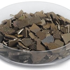
| Appearance/Color | Yellow-orange to brown solid. |
| Melting Point | 1,750 °C (3,180 °F; 2,020 K) 10 MPa |
| Density | 4.826 g/cm3 |
| Purity | 99.9% ~ 99.999% |
| Shape | Powder/ Granule/ Custom-made |
Applications
Cadmium sulfide evaporation materials are versatile and used in a variety of deposition techniques including:
- Semiconductor Deposition
- Chemical Vapor Deposition (CVD)
- Physical Vapor Deposition (PVD)
These materials are particularly useful in optics, serving purposes such as:
- Wear Protection
- Decorative Coatings
- Display Technologies
Packaging and Handling
To ensure quality and prevent damage, cadmium sulfide evaporation materials are carefully packaged with clear labeling for easy identification. This meticulous approach extends through storage and transportation to maintain the material’s integrity.
Contact Us
TFM is a leading provider of high-purity cadmium sulfide evaporation materials. We offer various forms including tablets, granules, rods, and wires, with options for custom shapes and quantities. Additionally, TFM supplies evaporation sources, boats, filaments, crucibles, heaters, and e-beam crucible liners. For pricing information or to request materials not listed, please reach out to us directly.


Reviews
There are no reviews yet.