 MSDS File
| Material Type | Carbon |
| Symbol | C |
| Atomic Weight | 12.0107 |
| Atomic Number | 6 |
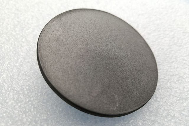
| Color/Appearance | Black, Non-Metallic |
| Thermal Conductivity | 140 W/m.K |
| Melting Point (°C) | ~3,652 |
| Coefficient of Thermal Expansion | 7.1 x 10⁻⁶/K |
| Theoretical Density (g/cc) | 2.25 |
| Z Ratio | 3.26 |
| Sputter | PDC |
| Max Power Density* (Watts/Square Inch) |
80 |
| Type of Bond | Indium, Elastomer |
| Comments | E-beam preferred. Arc evaporation. Poor film adhesion. |
Overview of Carbon Sputtering Targets
Introduction to Carbon Sputtering Targets
Carbon sputtering targets, symbolized as “C,” are widely utilized in thin-film deposition processes across various industries. Carbon, derived from the Latin word “carbo” meaning coal, is a non-metallic, tetravalent element with atomic number 6. It forms strong covalent chemical bonds and exhibits multiple allotropic forms, including graphite, diamond, and amorphous carbon. Each allotrope possesses unique physical properties that make carbon an invaluable material for advanced applications.
Key Properties of Carbon Sputtering Targets
- Material Type: Carbon
- Symbol: C
- Atomic Weight: 12.0107
- Atomic Number: 6
- Appearance: Black, non-metallic
- Thermal Conductivity: 140 W/m.K
- Melting Point: ~3,652°C
- Coefficient of Thermal Expansion: 7.1 × 10⁻⁶/K
- Density: 2.25 g/cc
- Z Ratio: 3.26
- Sputtering Method: PDC
- Max Power Density: 80 W/in²
- Bonding Options: Indium, Elastomer
Manufacturing Process
- Refining: Utilizing a three-layer electrolytic process to ensure high purity.
- Melting and Casting: Employing an electrical resistance furnace for semi-continuous casting.
- Grain Refinement: Achieving engineered microstructures through thermomechanical treatment.
- Final Packaging: Cleaned and prepared for vacuum use, with protection against environmental contaminants during shipping.
Product Specifications
- Purity: 99.99%–99.999%
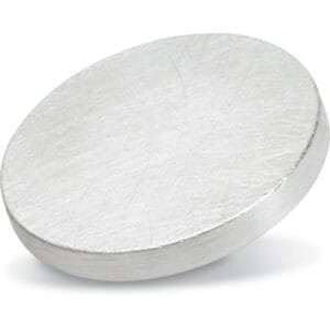
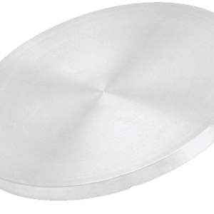
- Circular Dimensions: Up to 14-inch diameter, minimum 1 mm thickness.
- Block Dimensions: Up to 32-inch length, 12-inch width, minimum 1 mm thickness.
Features and Benefits
- High Purity: Ensures optimal performance for critical applications.
- Refined Grain Structure: Provides superior film quality and durability.
- Competitive Pricing: Offers cost-effective solutions for various industries.
- Semiconductor Grade: Suitable for advanced electronic and semiconductor applications.
Applications
Carbon sputtering targets are employed in:
- Electronics
- Semiconductor Fabrication
- Flat Panel Display Manufacturing
Additional Options
- Carbide Targets: Including Boron Carbide, Hafnium Carbide, Molybdenum Carbide, and more.
- Bonding Services: Indium and elastomer bonding to meet specific project needs.
Inquiry Form
Required Information
- Name
- Email ID
- Company Name
- Industry
Optional Information
- Phone Number
- Address
- Country
- Details About Material Requirements
Submit your inquiry to learn more about our carbon sputtering targets, or explore options tailored to your application needs.

Reviews
There are no reviews yet.