
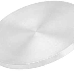
Cerium Boride Sputtering Target Description
A Cerium Boride Sputtering Target is a ceramic material composed of cerium and boron, used in sputtering processes. This type of target is commonly utilized in thin film deposition and other specialized applications due to its unique material properties.
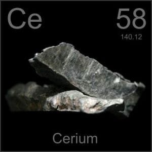 Cerium is a chemical element named after Ceres, the Roman goddess of agriculture. It was first identified in 1803 by scientists Martin Heinrich Klaproth, Jöns Jacob Berzelius, and Wilhelm Hisinger. The element was later isolated and its properties announced by Carl Gustaf Mosander. Cerium is represented by the symbol “Ce” and has an atomic number of 58. It is located in Period 6 and Group 3 of the periodic table, belonging to the f-block. The relative atomic mass of cerium is approximately 140.116 Daltons, with the number in parentheses indicating a margin of uncertainty.
Related Product: Cerium Sputtering Target
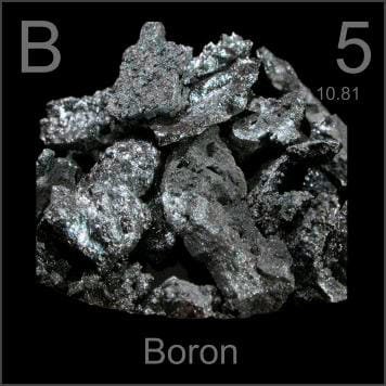 Boron is a chemical element with the symbol “B” and an atomic number of 5. The name “boron” derives from the Arabic word ‘buraq,’ referring to borax. The element was first identified in 1808 by scientists Louis-Joseph Gay-Lussac and Louis-Jacques Thénard. The isolation of boron was later achieved and announced by Sir Humphry Davy. Boron is located in Period 2 and Group 13 of the periodic table, classified under the p-block elements. Its relative atomic mass is approximately 10.811 Daltons, with the value in parentheses indicating a margin of uncertainty.
Cerium Boride Sputtering Target Application
The Cerium Boride Sputtering Target is utilized in a variety of applications, including thin film deposition and decorative coatings. It is commonly used in the semiconductor industry, display technologies, LED and photovoltaic device manufacturing, and functional coatings. Additionally, it plays a significant role in the optical information storage industry, glass coatings for automotive and architectural purposes, and optical communication technologies.
Cerium Boride Sputtering Target Packing
Our Cerium Boride Sputtering Targets are clearly tagged and labeled externally to facilitate easy identification and uphold stringent quality control measures. We take great care to protect these targets from damage during storage and transportation, ensuring they arrive in excellent condition.
Get Contact
TFM offers Cerium Boride Sputtering Targets in various forms, purities, sizes, and prices. We specialize in high-purity thin film deposition materials with optimal density and minimal grain sizes, which are ideal for semiconductor, CVD, and PVD applications in display and optics. Contact Us for current pricing on sputtering targets and other deposition materials that are not listed.


Reviews
There are no reviews yet.