Generic selectors
Exact matches only
Search in title
Search in content
Post Type Selectors

VD0777 Cesium Fluoride Evaporation Materials, CsF

Catalog No.VD0777
MaterialCesium Fluoride (CsF)
Purity99.9% ~ 99.99%
ShapePowder/ Granule/ Custom-made

TFM stands out as a premier manufacturer and supplier of high-purity Cesium Fluoride evaporation materials. Our extensive product range includes various evaporation materials, all available in powder and granule forms. For those with specific needs, we also offer customized forms upon request, ensuring that our solutions meet precise application requirements.

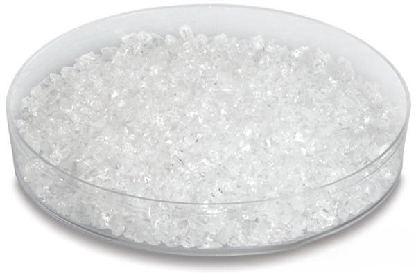
TFM: High-Purity Cesium Fluoride Evaporation Materials

TFM provides high-purity Cesium Fluoride (CsF) evaporation materials, known for their crucial role in achieving superior quality deposited films. Our CsF products, with a purity level of up to 99.9995%, are produced through stringent quality assurance processes to ensure maximum reliability and performance.

Cesium Fluoride Evaporation Materials Specification

Material TypeCesium Fluoride
SymbolCsF
Appearance/ColorWhite crystalline solid
Melting Point703 °C (1,297 °F; 976 K)
Density4.64 g/cm3
Purity99.9% ~ 99.99%
ShapePowder/ Granule/ Custom-made

Applications

Cesium Fluoride evaporation materials are versatile and used in various deposition techniques:

  • Semiconductor Deposition
  • Chemical Vapor Deposition (CVD)
  • Physical Vapor Deposition (PVD)

They are primarily applied in optics, including wear protection, decorative coatings, and displays.

Packaging

Our Cesium Fluoride materials are carefully packaged and labeled for clear identification and quality control. We ensure robust packaging to prevent any damage during storage and transportation.

Contact Us

TFM offers Cesium Fluoride in several forms, including tablets, granules, rods, and wires. Custom shapes and quantities are available upon request. Additionally, we provide related products such as evaporation sources, boats, filaments, crucibles, heaters, and e-beam crucible liners. For pricing and further inquiries, please contact us directly.

Reviews

There are no reviews yet.

Be the first to review “VD0777 Cesium Fluoride Evaporation Materials, CsF”

Your email address will not be published. Required fields are marked *

FAQ

  • They are high‐purity substances (e.g. metals, alloys, or compounds) used in thermal or electron‐beam evaporation processes to form thin films on substrates.

  • Typically, they’re processed into a form (often ingots, pellets, or wires) that can be efficiently vaporized. Preparation emphasizes high purity and controlled composition to ensure film quality.

  • Thermal evaporation and electron-beam (e-beam) evaporation are the two main techniques, where material is heated (or bombarded with electrons) until it vaporizes and then condenses on the substrate.

  • Thermal evaporation heats the material directly (often using a resistive heater), while e-beam evaporation uses a focused electron beam to locally heat and vaporize the source material—each method offering different control and energy efficiency.

  • Key parameters include source temperature, vacuum level, deposition rate, substrate temperature, and the distance between the source and the substrate. These factors influence film uniformity, adhesion, and microstructure.

  • Evaporation generally produces high-purity films with excellent control over thickness, and it is especially suitable for materials with relatively low melting points or high vapor pressures.

  • Challenges include issues with step coverage (due to line-of-sight deposition), shadowing effects on complex topographies, and possible re-evaporation of material from the substrate if temperature isn’t properly controlled.

  • Common evaporation materials include noble metals (e.g., gold, silver), semiconductors (e.g., silicon, germanium), metal oxides, and organic compounds—each chosen for its specific optical, electrical, or mechanical properties.

  • Selection depends on desired film properties (conductivity, optical transparency, adhesion), compatibility with the evaporation process, and the final device application (semiconductor, optical coating, etc.).

  • Optimizing substrate temperature, deposition rate, and chamber vacuum are critical for ensuring that the film adheres well and forms the intended microstructure without defects.

  • Troubleshooting may involve checking the source material’s purity, ensuring stable source temperature, verifying the vacuum level, adjusting the substrate’s position or temperature, and monitoring deposition rate fluctuations.

While evaporation tends to yield very high purity films with excellent thickness control, it is limited by its line-of-sight nature. In contrast, sputtering can deposit films more uniformly on complex surfaces and is more versatile for a broader range of materials.


Shopping Cart
Scroll to Top