 MSDS File
Chromium Diboride Evaporation Materials Overview
Chromium diboride (CrB₂) is a key material used in high-precision deposition processes, offering exceptional quality for film deposition applications. TFM specializes in providing chromium diboride with an impressive purity level of up to 99.9995%. This high purity is essential for ensuring the reliability and quality of deposited films in various high-tech applications.
Specifications
| Material Type | Chromium diboride |
| Symbol | AlB2 |
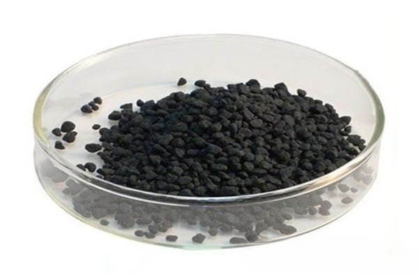
| Appearance/Color | Solid |
| Melting Point | 1,950 to 2,050 °C (3,540 to 3,720 °F; 2,220 to 2,320 K) |
| Density | 6.17 g/cm3 |
| Purity | 99.9% |
| Shape | Powder/ Granule/ Custom-made |
Applications
Chromium diboride evaporation materials are integral to several deposition techniques, including:
- Semiconductor Deposition
- Chemical Vapor Deposition (CVD)
- Physical Vapor Deposition (PVD)
These materials are predominantly used in optical coatings, such as wear-resistant layers, decorative finishes, and display technologies.
Packaging and Handling
To ensure the highest standards of quality and prevent damage, chromium diboride evaporation materials are carefully tagged, labeled, and packed. This meticulous approach aids in maintaining product integrity during storage and transportation.
Contact Information
TFM is a premier provider of high-purity chromium diboride evaporation materials, available in various forms such as tablets, granules, rods, and wires. We also offer custom solutions tailored to your specific needs. In addition to chromium diboride, TFM supplies a range of evaporation sources, including boats, filaments, crucibles, heaters, and e-beam crucible liners. For up-to-date pricing and availability of both listed and custom materials, please contact us directly with your inquiry.


Reviews
There are no reviews yet.