 MSDS File
TFM: Premium Chromium(III) Fluoride Evaporation Materials
TFM specializes in high-purity Chromium(III) Fluoride (CrF3) evaporation materials, essential for achieving high-quality deposited films. Our Chromium(III) Fluoride products are manufactured with purity levels up to 99.9995%, thanks to rigorous quality control processes that ensure superior performance and reliability.
Chromium(III) Fluoride Evaporation Materials Specification
| Material Type | Chromium(III) Fluoride |
| Symbol | CrF3 |
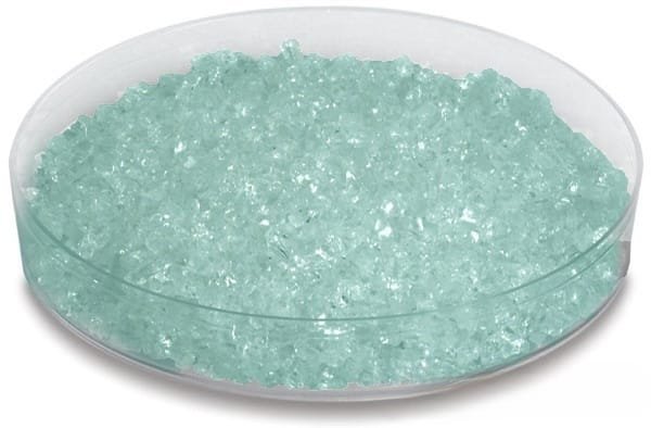
| Appearance/Color | Green crystalline solid |
| Melting Point | 1,100 °C (2,010 °F; 1,370 K) (sublimes) |
| Density | 3.8 g/cm3 (anhydrous) 2.2 g/cm3 (trihydrate) |
| Purity | 99.9% |
| Shape | Powder/ Granule/ Custom-made |
Applications
Chromium(III) Fluoride evaporation materials are versatile and used in:
- Semiconductor Deposition
- Chemical Vapor Deposition (CVD)
- Physical Vapor Deposition (PVD)
These materials are also employed in optics for wear protection, decorative coatings, and displays.
Packaging
Our Chromium(III) Fluoride materials are meticulously tagged and labeled to ensure proper identification and quality control. We take special care to prevent any damage during storage and transport.
Contact Us
TFM offers Chromium(III) Fluoride in various forms, including tablets, granules, rods, and wires. Custom shapes and quantities are available upon request. Additionally, we provide related products such as evaporation sources, boats, filaments, crucibles, heaters, and e-beam crucible liners. For current pricing and additional inquiries, please contact us directly.


Reviews
There are no reviews yet.