 MSDS File
Chromium Nickel Evaporation Materials
Introduction
Chromium Nickel evaporation materials are widely used in thin film deposition due to their exceptional combination of mechanical strength, corrosion resistance, and electrical properties. By blending chromium’s hardness and oxidation resistance with nickel’s ductility and conductivity, these evaporation sources enable the production of thin films that meet demanding requirements in electronics, optics, and protective coatings.
Detailed Description
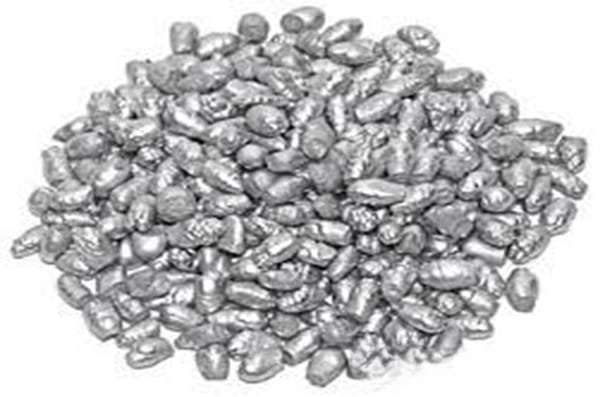
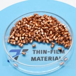
Chromium Nickel evaporation materials are typically prepared in pellet, granule, or custom-formed pieces suitable for thermal and electron beam evaporation systems. The alloy is engineered for high-density and uniform composition, ensuring stable evaporation behavior and consistent thin film properties.
Purity: Offered in 99.9% and higher for reduced contamination in critical thin film applications.
Composition: Standard Cr-Ni alloy ratios are available, with customization possible to meet specific optical, mechanical, or electronic requirements.
Deposition Stability: Designed to minimize spitting and provide uniform evaporation rates, which is critical for achieving defect-free coatings.
Film Properties: Films deposited from Chromium Nickel exhibit high adhesion, durability, and good thermal stability, making them suitable for harsh environments.
Applications
Chromium Nickel evaporation materials find applications in multiple industries:
Semiconductors – barrier layers and diffusion control.
Optical coatings – anti-reflective and decorative finishes.
Protective coatings – wear-resistant and corrosion-resistant layers.
Aerospace & automotive – durable coatings for components exposed to high stress and temperature.
Energy technologies – electrode materials in batteries and thin film solar cells.
Technical Parameters
| Parameter | Typical Value / Range | Importance |
|---|---|---|
| Purity | 99.9% – 99.99% | Ensures film quality and reduces contamination |
| Forms Available | Pellets, granules, custom pieces | Compatible with e-beam and thermal evaporation |
| Size Range | 1 – 20 mm (pellets/granules) | Affects evaporation rate stability |
| Evaporation Method | Thermal / Electron beam | Enables flexible coating processes |
| Composition | Cr-Ni alloys (custom ratios) | Tailors film hardness and conductivity |
Comparison with Related Materials
| Material | Key Advantage | Typical Application |
|---|---|---|
| Chromium Nickel (Cr-Ni) | Balanced corrosion resistance & mechanical strength | Protective & optical coatings |
| Pure Chromium | Excellent hardness & oxidation resistance | Decorative & wear coatings |
| Pure Nickel | High conductivity & ductility | Electronic & magnetic films |
| Nickel Iron (Ni-Fe) | Soft magnetic properties | Magnetic thin films |
FAQ
| Question | Answer |
|---|---|
| Can the Cr:Ni ratio be customized? | Yes, alloy composition can be tailored for specific thin film performance. |
| What deposition methods are compatible? | Suitable for thermal and electron beam evaporation systems. |
| How are these materials packaged? | Vacuum-sealed with inert gas protection, then packed in export-safe cartons or crates. |
| What purity levels are offered? | Typically 3N (99.9%) to 4N (99.99%) depending on requirements. |
| Which industries benefit most? | Semiconductor, optics, aerospace, automotive, and renewable energy. |
Packaging
Chromium Nickel evaporation materials are vacuum-sealed and protected with inert gas to prevent oxidation during storage and shipping. They are securely packed with protective foam and placed in export-approved cartons or wooden crates to ensure safe arrival.
Conclusion
Chromium Nickel evaporation materials deliver a reliable combination of durability, conductivity, and corrosion resistance, making them ideal for advanced thin film applications. With customizable compositions and forms, they provide tailored solutions for research and industrial production.
For detailed specifications and a quotation, please contact us at [sales@thinfilmmaterials.com].


Reviews
There are no reviews yet.