
 MSDS File
Product Overview
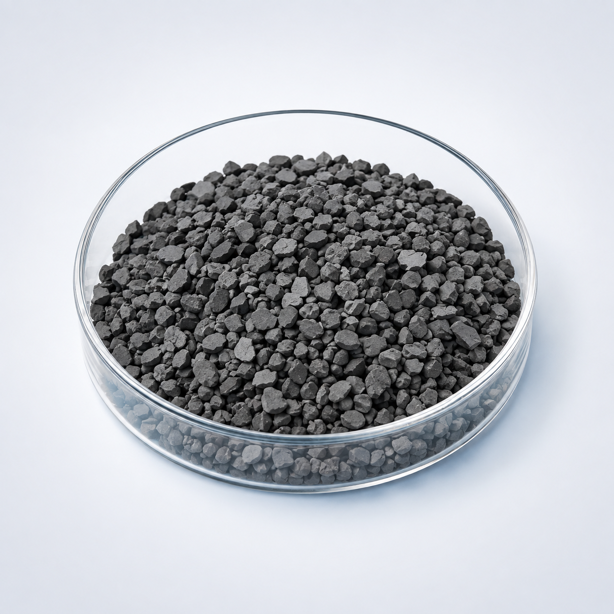
CIGS(CuInxGa1-xSe2) Pellet Evaporation Material (CuInxGa1-xSe2) is supplied in pellet form to provide a compact, controlled charge for evaporation research involving complex or multicomponent materials. Pellet geometry can improve loading and handling, but it does not guarantee congruent evaporation. For multicomponent semiconductors and chalcogenides, the relative vapor pressures of the constituents, heating method, and deposition rate can influence film composition.
Evaporation Behavior and Process Considerations
Pellets should be loaded so that the charge is mechanically stable and heats uniformly. For complex materials, a slow preconditioning step can reduce trapped gas release and thermal shock. Because multicomponent pellets may not evaporate congruently, quartz-crystal rate monitoring alone should not be treated as proof of final film stoichiometry.
Technical Data
| Parameter | Typical Value / Range | Importance |
|---|---|---|
| Purity | 99.9% – 99.99% | Ensures minimal contamination |
| Composition | CuInₓGa₁₋ₓSe₂ (ₓ adjustable 0–1) | Bandgap control for solar efficiency |
| Form | Pellet | Stable for evaporation sources |
| Particle Size | 3 – 12 mm (customizable) | Matches crucible/e-beam needs |
| Bandgap Range | 1.0 – 1.7 eV | Optimized for photovoltaic applications |
| Material | Key Advantage | Typical Application |
|---|---|---|
| CIGS (CuInₓGa₁₋ₓSe₂) | Tunable bandgap, high efficiency | Thin film solar cells |
| CIS (CuInSe₂) | Narrow bandgap (~1.0 eV) | Low-bandgap PV, R&D |
| CGS (CuGaSe₂) | Wider bandgap (~1.7 eV) | Tandem PV, optoelectronics |
| Question | Answer |
|---|---|
| Can the In/Ga ratio be customized? | Yes, the composition can be tailored to achieve desired bandgaps. |
| What deposition methods are suitable? | Both e-beam evaporation and thermal evaporation are applicable. |
| Is this material used in commercial solar modules? | Yes, CIGS is one of the leading thin film absorber materials in industry. |
| How is it packaged? | Vacuum-sealed in moisture-protected containers, shipped in export-safe cartons or wooden crates. |
| What industries benefit most? | Photovoltaic manufacturing, optoelectronics, and semiconductor research. |
Typical Thin-Film Applications
- Thin-film R&D requiring a composition-specific evaporation source
- Optical, semiconductor, electronic, energy, and advanced-material coating studies depending on the compound
- Custom PVD research using pellets, pieces, granules, or other source forms
Source Form and Ordering Considerations
For quotation, provide the material or formula, purity, desired source form and size, quantity, evaporation method if known, and any crucible, boat, or e-beam hearth constraints. For compound materials, include the target film composition or application when possible so that source form and process risk can be reviewed together. TFM can supply pellets, pieces, granules, tablets, or other custom forms subject to material manufacturability.
Frequently Asked Questions
Why is CIGS(CuInxGa1-xSe2) Pellet supplied as an evaporation pellet?
Pelletizing provides a compact charge that is easier to load, handle, and heat than loose powder. It also helps reduce dust and movement inside the source holder.
Does a CIGS(CuInxGa1-xSe2) Pellet pellet evaporate congruently?
Not necessarily. In multicomponent materials, individual elements can have different vapor pressures, so the film can drift from the nominal pellet composition during deposition.
Should complex evaporation pellets be preconditioned?
Yes. A slow preheating step can reduce trapped gas release, thermal shock, and sudden spitting before the substrate shutter is opened.
Is e-beam evaporation suitable for CIGS(CuInxGa1-xSe2) Pellet pellets?
It can be, especially when localized heating is needed, but suitability depends on decomposition behavior, electrical/thermal properties, and the desired film composition.
How should the final film composition be controlled?
Use deposition-rate control together with post-deposition composition analysis. For strict composition tolerances, co-evaporation from separately controlled sources may be considered.
What dimensions can be customized for CIGS(CuInxGa1-xSe2) Pellet pellets?
Pellet diameter, thickness, charge mass, and quantity can be reviewed according to the source pocket or crucible dimensions and material manufacturability.
Reviews
There are no reviews yet.