 MSDS File
Introduction
Copper evaporation materials are widely used in thin film deposition processes due to copper’s excellent electrical conductivity, thermal conductivity, and adhesion properties. These materials are indispensable in industries such as semiconductors, data storage, optics, and energy devices, where high-quality copper films are required to ensure performance and reliability.
Detailed Description
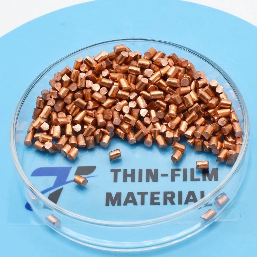
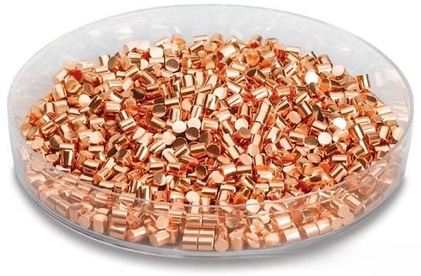
Our copper evaporation materials are produced using high-purity copper refined through advanced vacuum melting and shaping processes. The materials are available in multiple forms, including pellets, shots, granules, wires, and custom-shaped pieces, designed to suit various evaporation systems.
The purity of copper (typically 99.9%–99.999%) directly affects the conductivity and uniformity of thin films, making it critical for demanding applications. Shape and size uniformity are carefully controlled to ensure stable evaporation rates, while optional granule or pellet forms help minimize spitting during heating.
For thermal and electron beam evaporation systems, copper evaporation materials demonstrate stable vapor pressure and consistent deposition behavior, enabling precise control of thin film thickness and microstructure.
Applications
Copper evaporation materials are applied across a broad spectrum of industries, including:
Semiconductor fabrication – interconnects, seed layers, and diffusion barriers.
Optical coatings – reflective layers in optics and display devices.
Data storage – magnetic recording media.
Decorative coatings – jewelry, watch components, and architectural finishes.
Energy devices – thin film solar cells, batteries, and fuel cells.
Technical Parameters
| Parameter | Typical Value / Range | Importance |
|---|---|---|
| Purity | 99.9% – 99.999% (3N–5N) | Higher purity ensures conductivity & fewer defects |
| Forms Available | Pellets, shots, granules, wire, custom | Compatible with various evaporation sources |
| Size Range | 1–20 mm (pellets/granules) | Influences evaporation stability |
| Evaporation Method | Thermal / E-beam | Choice depends on film requirements |
| Packing | Vacuum sealed, inert gas protected | Prevents oxidation and contamination |
Comparison with Related Materials
| Material | Key Advantage | Typical Application |
|---|---|---|
| Copper (Cu) | High conductivity, good adhesion | Electronics, optics |
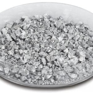
| Silver (Ag) | Highest conductivity, reflective | Mirrors, sensors |
| Aluminum (Al) | Lightweight, cost-effective | General coatings |
| Gold (Au) | Excellent corrosion resistance | High-end electronics, optics |
FAQ
| Question | Answer |
|---|---|
| Can copper evaporation materials be customized? | Yes, forms, sizes, and purity levels can be tailored for specific deposition systems. |
| What purity levels are available? | From 3N (99.9%) to 5N (99.999%) depending on application needs. |
| How are they packaged? | Vacuum-sealed in inert atmospheres with protective containers to avoid oxidation. |
| What deposition methods are compatible? | Suitable for thermal evaporation and electron beam evaporation systems. |
| Which industries use copper evaporation materials most? | Semiconductor, optics, decorative coatings, and renewable energy sectors. |
Packaging
Copper evaporation materials are carefully sealed in vacuum or inert gas environments to protect against oxidation. They are labeled with batch numbers, purity grades, and form specifications for traceability. Export packaging includes protective foam and reinforced cartons or wooden crates, ensuring safe transport and storage.
Conclusion
Copper evaporation materials deliver excellent film uniformity, conductivity, and adhesion, making them a reliable choice for advanced thin film deposition. With customizable forms and purities, they meet the diverse needs of research and industry.
For detailed specifications and a quotation, please contact us at [sales@thinfilmmaterials.com].


Reviews
There are no reviews yet.