
Introduction
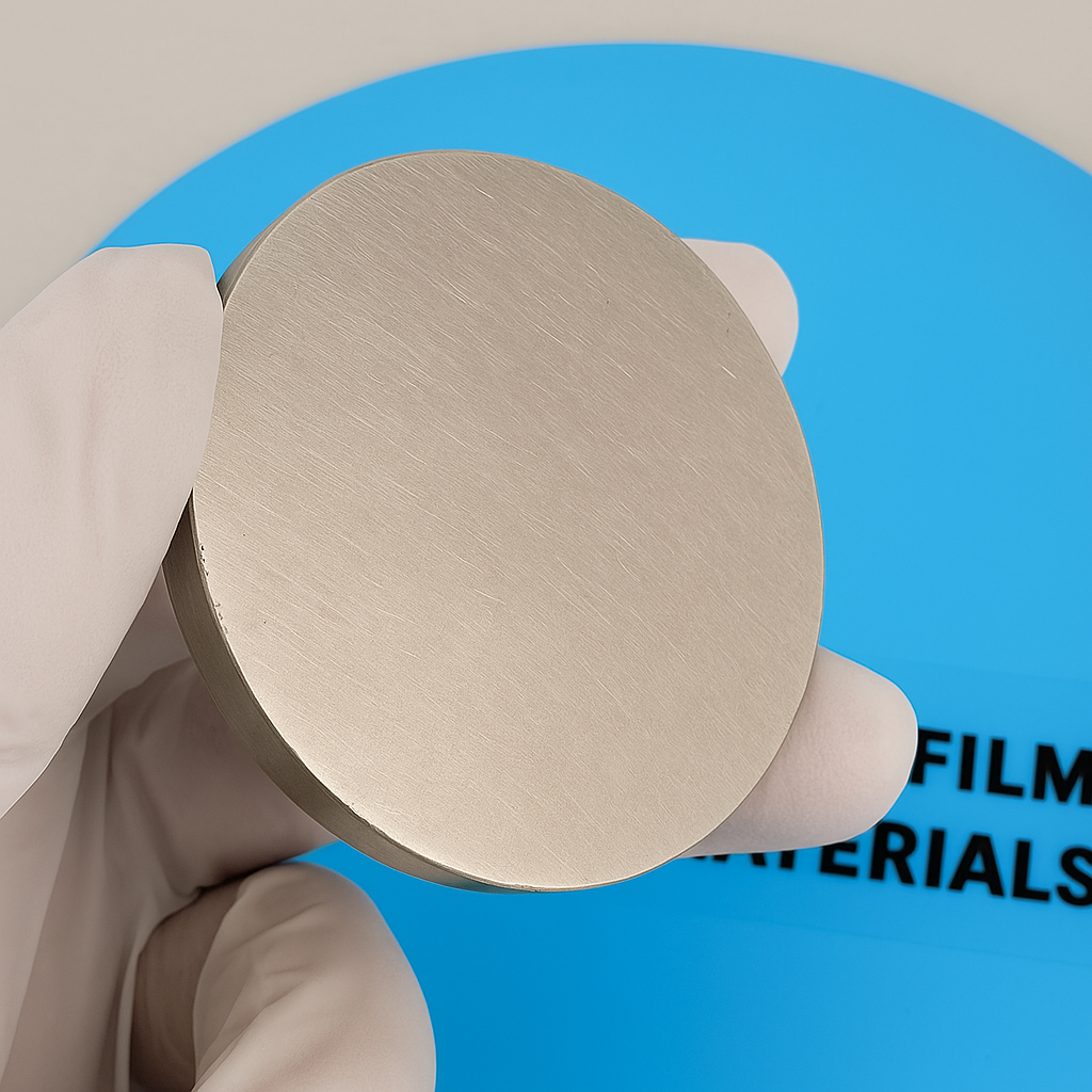
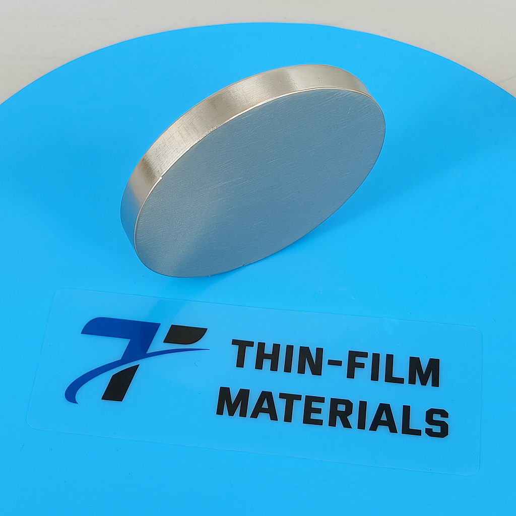
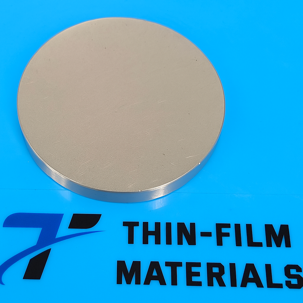
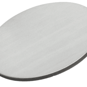
The Copper Gallium Sputtering Target (Cu/Ga) is a specialized alloy target widely used in thin film deposition processes for advanced semiconductor and photovoltaic applications. Copper and gallium are key components in several compound semiconductor systems, particularly in the production of CIGS (Copper Indium Gallium Selenide) thin-film solar cells. Through magnetron sputtering or other physical vapor deposition (PVD) methods, Cu/Ga targets enable the controlled deposition of precursor layers that contribute to high-efficiency photovoltaic materials.
Because of its tunable composition and compatibility with other semiconductor elements, the Cu/Ga sputtering target is widely utilized in solar energy technologies, optoelectronic devices, and advanced materials research.
Detailed Description
Copper Gallium sputtering targets are manufactured using high-purity copper and gallium through advanced metallurgical processes such as vacuum melting, alloy casting, or powder metallurgy. These methods ensure a homogeneous alloy structure with controlled composition, which is critical for maintaining stable sputtering behavior and producing uniform thin films.
Copper provides excellent electrical conductivity and forms the structural backbone of many semiconductor compounds, while gallium contributes important electronic and band-structure characteristics when combined with other elements such as indium and selenium. In thin film deposition systems, Cu/Ga targets are frequently used as precursor sources to control the copper-to-gallium ratio in compound semiconductor films.
In photovoltaic manufacturing, controlling the gallium concentration is particularly important because it directly influences the bandgap of the resulting absorber layer. Adjusting the Cu/Ga ratio allows researchers and manufacturers to tailor the optical absorption properties and improve device efficiency.
High-density Cu/Ga targets help ensure consistent sputtering rates, stable plasma conditions, and minimal particle generation. For high-power sputtering systems, targets can also be supplied with copper backing plates bonded using indium or diffusion bonding techniques, which improve heat dissipation and mechanical stability during deposition.
Applications
Copper Gallium sputtering targets are widely used in several advanced technology sectors:
Thin-film photovoltaic cells, particularly CIGS solar cell absorber layers
Compound semiconductor deposition for optoelectronic devices
Photovoltaic research and development focused on bandgap engineering
Optical and electronic thin films used in specialized semiconductor devices
Energy technology development involving advanced solar materials
Academic and industrial R&D laboratories studying chalcogenide semiconductors
Technical Parameters
| Parameter | Typical Value / Range | Importance |
|---|---|---|
| Purity | 99.9% – 99.99% | High purity ensures stable semiconductor properties |
| Composition | Cu/Ga ratios customizable (e.g., 90/10, 80/20) | Controls film composition and device performance |
| Diameter | 25 – 300 mm (custom) | Compatible with common sputtering systems |
| Thickness | 3 – 6 mm | Influences sputtering rate and target lifespan |
| Density | ≥ 99% theoretical density | Improves film uniformity and sputtering stability |
| Bonding | Copper backing plate / Indium bonded | Enhances thermal conductivity and structural stability |
Comparison with Related Materials
| Material | Key Advantage | Typical Application |
|---|---|---|
| Copper Gallium (Cu/Ga) | Adjustable alloy composition for semiconductor films | CIGS solar cell precursor layers |
| Copper (Cu) | Excellent electrical conductivity | Conductive thin films and electrodes |
| Gallium (Ga) | Semiconductor bandgap tuning | Compound semiconductor materials |
FAQ
| Question | Answer |
|---|---|
| Can the Cu/Ga composition be customized? | Yes. The copper-to-gallium ratio can be adjusted to meet specific photovoltaic or semiconductor deposition requirements. |
| Are bonded sputtering targets available? | Yes. Copper backing plates with indium bonding are commonly used to improve thermal conductivity and target durability. |
| What sputtering methods are suitable for Cu/Ga targets? | Cu/Ga sputtering targets are typically used in DC magnetron sputtering and other PVD deposition techniques. |
| What purity levels are typically available? | Standard purity ranges from 99.9% to 99.99%, depending on application needs. |
| Can the target size be customized? | Yes. Targets can be manufactured in a wide range of diameters, thicknesses, and geometries for different deposition systems. |
Packaging
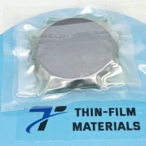
Our Copper Gallium Sputtering Target (Cu/Ga) products are meticulously tagged and labeled externally to ensure efficient identification and maintain strict quality control. Each target is carefully packaged using vacuum-sealed bags, protective foam materials, and export-grade cartons or wooden crates. These packaging methods protect the targets from contamination, oxidation, and mechanical damage during storage and transportation.
Conclusion
The Copper Gallium Sputtering Target (Cu/Ga) provides a reliable and versatile material solution for thin film deposition in photovoltaic and semiconductor technologies. Its adjustable composition allows precise control over film properties, making it particularly valuable for CIGS solar cell manufacturing and advanced compound semiconductor research.
With high purity levels, customizable compositions, and stable sputtering performance, Cu/Ga sputtering targets support the development of next-generation energy and electronic devices.
For detailed specifications and a quotation, please contact us at sales@thinfilmmaterials.com.

Reviews
There are no reviews yet.