Generic selectors
Exact matches only
Search in title
Search in content
Post Type Selectors

VD0843 Copper Indium Gallium Selenide (CIGS) Evaporation Materials

Catalog No.VD0843
MaterialCopper Indium Gallium Selenide (CIGS)
Purity99.9% ~ 99.999%
ShapePowder/ Granule/ Custom-made

TFM is a top-tier producer and distributor of premium-quality copper indium gallium selenide (CIGS) evaporation materials. In addition to CIGS, we supply a diverse range of other high-purity evaporation materials to meet the demands of various industries. Our materials come in both powder and granule forms, with the option for customized formats tailored to specific needs upon request.

Copper Indium Gallium Selenide (CIGS) Evaporation Materials Overview

TFM specializes in providing copper indium gallium selenide (CIGS) evaporation materials, a semiconductor compound made up of copper, indium, gallium, and selenium, with the chemical formula CuInGaSe (CIGS). This high-purity material is essential for deposition processes to create high-quality thin films. With purities reaching up to 99.9995%, TFM ensures that our CIGS evaporation materials are produced under strict quality control measures for maximum reliability.

Related Products:

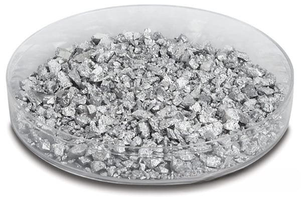
Specifications of Copper Indium Gallium Selenide (CIGS) Evaporation Materials

Material TypeCopper Indium Gallium Selenide
SymbolCuIn1−xGaxSe2  (x = 0–1)
Appearance/ColorSilvery
Melting Point990-1070 °C
Density~5.7 g/cm
Purity99.9% ~ 99.999%
ShapePowder/ Granule/ Custom-made

Applications of Copper Indium Gallium Selenide (CIGS) Evaporation Materials

CIGS evaporation materials are widely used in various deposition techniques, such as semiconductor deposition, chemical vapor deposition (CVD), and physical vapor deposition (PVD). Key applications include:

  • Optics: Display manufacturing, decorative coatings, and protective wear layers.

Packaging and Quality Control

To maintain product integrity, TFM ensures that all CIGS evaporation materials are securely labeled and packaged for easy identification and safe handling. This careful packaging process minimizes any risk of damage during transport or storage.

Custom Solutions and Contact Information

As a leading supplier of high-purity CIGS evaporation materials, TFM offers a wide range of shapes, including tablets, granules, rods, and wires. We also provide custom solutions tailored to your specific project requirements. In addition to CIGS materials, we supply a variety of evaporation sources, such as boats, filaments, crucibles, heaters, and e-beam crucible liners.

For pricing inquiries or more information on products not listed, feel free to contact us for a custom quote.

Reviews

There are no reviews yet.

Be the first to review “VD0843 Copper Indium Gallium Selenide (CIGS) Evaporation Materials”

Your email address will not be published. Required fields are marked *

FAQ

  • They are high‐purity substances (e.g. metals, alloys, or compounds) used in thermal or electron‐beam evaporation processes to form thin films on substrates.

  • Typically, they’re processed into a form (often ingots, pellets, or wires) that can be efficiently vaporized. Preparation emphasizes high purity and controlled composition to ensure film quality.

  • Thermal evaporation and electron-beam (e-beam) evaporation are the two main techniques, where material is heated (or bombarded with electrons) until it vaporizes and then condenses on the substrate.

  • Thermal evaporation heats the material directly (often using a resistive heater), while e-beam evaporation uses a focused electron beam to locally heat and vaporize the source material—each method offering different control and energy efficiency.

  • Key parameters include source temperature, vacuum level, deposition rate, substrate temperature, and the distance between the source and the substrate. These factors influence film uniformity, adhesion, and microstructure.

  • Evaporation generally produces high-purity films with excellent control over thickness, and it is especially suitable for materials with relatively low melting points or high vapor pressures.

  • Challenges include issues with step coverage (due to line-of-sight deposition), shadowing effects on complex topographies, and possible re-evaporation of material from the substrate if temperature isn’t properly controlled.

  • Common evaporation materials include noble metals (e.g., gold, silver), semiconductors (e.g., silicon, germanium), metal oxides, and organic compounds—each chosen for its specific optical, electrical, or mechanical properties.

  • Selection depends on desired film properties (conductivity, optical transparency, adhesion), compatibility with the evaporation process, and the final device application (semiconductor, optical coating, etc.).

  • Optimizing substrate temperature, deposition rate, and chamber vacuum are critical for ensuring that the film adheres well and forms the intended microstructure without defects.

  • Troubleshooting may involve checking the source material’s purity, ensuring stable source temperature, verifying the vacuum level, adjusting the substrate’s position or temperature, and monitoring deposition rate fluctuations.

While evaporation tends to yield very high purity films with excellent thickness control, it is limited by its line-of-sight nature. In contrast, sputtering can deposit films more uniformly on complex surfaces and is more versatile for a broader range of materials.


Shopping Cart
Scroll to Top