Generic selectors
Exact matches only
Search in title
Search in content
Post Type Selectors

VD0682 Copper(II) Oxide Evaporation Materials, CuO

Catalog No.VD0682
MaterialCopper Oxide (CuO)
Purity99.9% ~ 99.99%
ShapePowder/ Granule/ Custom-made
TFM is a premier producer and provider of high-purity copper(II) oxide evaporation materials, along with a diverse selection of other evaporation materials. Our offerings include both powder and granule forms, and we also accommodate custom orders to meet specific needs.

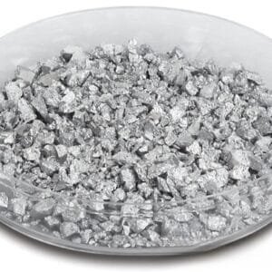
Copper(II) Oxide Evaporation Materials Overview

Copper(II) oxide evaporation materials, with the chemical formula CuO, are integral to achieving superior film deposition quality. TFM specializes in manufacturing copper(II) oxide with exceptional purity, up to 99.9995%, ensuring reliable performance in various applications.

Product Specifications

Material Type Copper(II) Oxide
Form Evaporation Materials
Symbol CuO
Color/Appearance Black to brown
Melting Point1,326 °C
Density6.315 g/cm3
Purity 99.5% ~ 99.99%
Shape Powder/ Granule/ Custom-made

Applications

Copper(II) oxide evaporation materials serve multiple purposes:

  • Deposition Processes: Vital for semiconductor deposition, chemical vapor deposition (CVD), and physical vapor deposition (PVD).
  • Optical Uses: Utilized in protective coatings, decorative finishes, and display technologies.

Packaging and Handling

Our copper(II) oxide materials are meticulously packaged with clear labeling to ensure easy identification and rigorous quality control. We take great care to prevent damage during storage and transportation.

Contact Us

TFM is a leading provider of high-purity copper(II) oxide evaporation materials, available in various forms including tablets, granules, rods, and wires. Custom shapes and quantities can also be accommodated. In addition to evaporation materials, we offer evaporation sources, boats, filaments, crucibles, heaters, and e-beam crucible liners. For up-to-date pricing and information on additional products, please contact us directly.

For further inquiries or to request a quote, please reach out to us.

Reviews

There are no reviews yet.

Be the first to review “VD0682 Copper(II) Oxide Evaporation Materials, CuO”

Your email address will not be published. Required fields are marked *

FAQ

  • They are high‐purity substances (e.g. metals, alloys, or compounds) used in thermal or electron‐beam evaporation processes to form thin films on substrates.

  • Typically, they’re processed into a form (often ingots, pellets, or wires) that can be efficiently vaporized. Preparation emphasizes high purity and controlled composition to ensure film quality.

  • Thermal evaporation and electron-beam (e-beam) evaporation are the two main techniques, where material is heated (or bombarded with electrons) until it vaporizes and then condenses on the substrate.

  • Thermal evaporation heats the material directly (often using a resistive heater), while e-beam evaporation uses a focused electron beam to locally heat and vaporize the source material—each method offering different control and energy efficiency.

  • Key parameters include source temperature, vacuum level, deposition rate, substrate temperature, and the distance between the source and the substrate. These factors influence film uniformity, adhesion, and microstructure.

  • Evaporation generally produces high-purity films with excellent control over thickness, and it is especially suitable for materials with relatively low melting points or high vapor pressures.

  • Challenges include issues with step coverage (due to line-of-sight deposition), shadowing effects on complex topographies, and possible re-evaporation of material from the substrate if temperature isn’t properly controlled.

  • Common evaporation materials include noble metals (e.g., gold, silver), semiconductors (e.g., silicon, germanium), metal oxides, and organic compounds—each chosen for its specific optical, electrical, or mechanical properties.

  • Selection depends on desired film properties (conductivity, optical transparency, adhesion), compatibility with the evaporation process, and the final device application (semiconductor, optical coating, etc.).

  • Optimizing substrate temperature, deposition rate, and chamber vacuum are critical for ensuring that the film adheres well and forms the intended microstructure without defects.

  • Troubleshooting may involve checking the source material’s purity, ensuring stable source temperature, verifying the vacuum level, adjusting the substrate’s position or temperature, and monitoring deposition rate fluctuations.

While evaporation tends to yield very high purity films with excellent thickness control, it is limited by its line-of-sight nature. In contrast, sputtering can deposit films more uniformly on complex surfaces and is more versatile for a broader range of materials.


Shopping Cart
Scroll to Top