 MSDS File
Introduction
Copper Selenide Evaporation Materials are compound chalcogenide materials widely used in thin film deposition for semiconductor, optoelectronic, and energy-related applications. With well-defined copper–selenium stoichiometry and favorable electronic properties, copper selenide is an important source material for research and production processes involving compound semiconductor and functional thin films.
Detailed Description
Copper selenide evaporation materials are produced from high-purity copper and selenium through carefully controlled synthesis and consolidation processes to ensure accurate stoichiometry and compositional uniformity. Precise control of phase composition—such as Cu₂Se or related Cu–Se phases—is essential, as it directly affects electrical conductivity, carrier concentration, and optical behavior in deposited films.
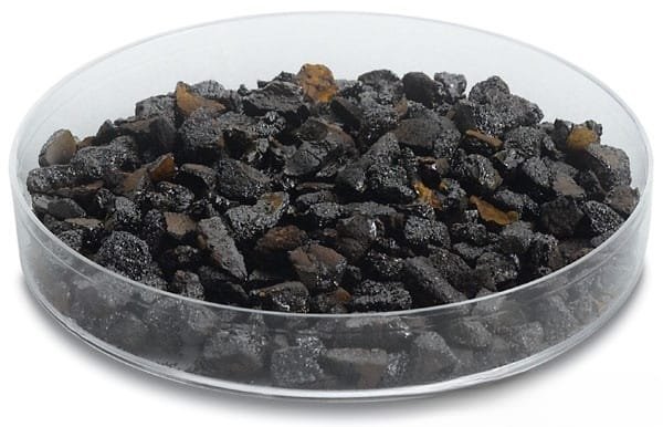
These materials are supplied in forms suitable for thermal evaporation and electron-beam (e-beam) evaporation, including pellets, granules, and pieces. Optimized particle size and surface condition help ensure smooth melting behavior, stable evaporation rates, and reduced spitting during deposition. Copper selenide evaporation materials are compatible with a wide range of crucibles and liners commonly used in PVD systems.
Customized compositions, forms, and batch sizes are available to support both exploratory laboratory research and repeatable industrial coating processes.
Applications
Compound semiconductor thin films
Photovoltaic and energy conversion research
Optoelectronic and infrared devices
Functional chalcogenide coatings
Thin film materials research and development
Technical Parameters
| Parameter | Typical Value / Range | Importance |
|---|---|---|
| Material | Copper Selenide (Cu–Se) | Compound semiconductor source |
| Stoichiometry | Cu₂Se or custom Cu/Se ratio | Controls electrical & optical properties |
| Purity | 99.9% – 99.99% | Impurity control affects film quality |
| Form | Pellets, granules, pieces | Compatible with evaporation sources |
| Evaporation Method | Thermal / E-beam evaporation | Process flexibility |
| Packaging | Vacuum-sealed, inert protected | Prevents oxidation & contamination |
Comparison with Related Evaporation Materials
| Material | Key Advantage | Typical Application |
|---|---|---|
| Copper Selenide | Balanced conductivity & band structure | Semiconductor & PV films |
| Copper Sulfide | Strong optical absorption | Photovoltaics |
| Zinc Selenide | Wide bandgap | Optoelectronics & optics |
FAQ
| Question | Answer |
|---|---|
| Can the Cu/Se ratio be customized? | Yes, stoichiometry can be tailored to your deposition requirements. |
| Is copper selenide suitable for thermal evaporation? | Yes, it is commonly used in both thermal and e-beam evaporation systems. |
| How is compositional uniformity ensured? | Through controlled synthesis and strict quality inspection. |
| How is the material packaged? | Vacuum-sealed or packed under inert atmosphere to maintain purity. |
| Is a Certificate of Analysis available? | Yes, CoA is provided upon request. |
Packaging
Our Copper Selenide Evaporation Materials are carefully weighed, labeled, and sealed under vacuum or inert atmosphere to protect against oxidation and moisture. Protective inner packaging and export-grade outer cartons ensure safe storage and international transportation.
Conclusion
Copper Selenide Evaporation Materials provide reliable composition control, stable evaporation behavior, and flexible form options for advanced thin film deposition. With consistent quality and customizable specifications, they are well suited for semiconductor, optoelectronic, and energy-focused PVD applications.
For detailed specifications and a quotation, please contact us at sales@thinfilmmaterials.com.


Reviews
There are no reviews yet.