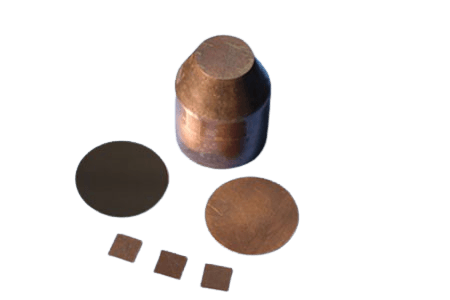
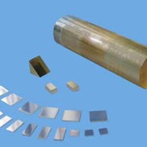
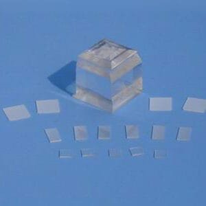
Copper Substrate
Copper (Cu) single crystal substrates are extensively used in a variety of applications, including matrix metals, alloy films, and biomaterials. These substrates offer superior thermal and electrical conductivity, making them ideal for demanding electronic and industrial uses. Manufactured through the Bridgman method, they exhibit high purity and precise crystalline orientation, ensuring reliable performance in advanced applications.
Physical Properties of Copper Substrate
| Property | Value |
|---|---|
| Material | Copper |
| Crystal Structure | M3 |
| Growth Method | Bridgman Method |
| Lattice (Å) | a = 3.607 |
| Density (g/cm³) | Dx = 8.989; Dm = 8.95 |
| Purity | > 4N |
| Melting Point (℃) | 1083 |
Specifications
- Standard Sizes: 10×3, 10×5, 10×10, 15×15, 20×15, 20×20 mm
- Customization: Available on demand
- Thickness: 0.5 mm, 1.0 mm
- Crystal Orientation: <100>, <110>, <111>
- Polish Options: SSP or DSP
- Redirection Precision: ±0.5°
- Redirection of Edge: 2° (special in 1°)
- Angle of Crystalline: Available on request
- Surface Roughness (Ra): ≤5Å (5µm×5µm)
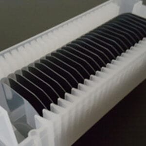
Copper Substrate Packaging
- Packaged in class 100 clean bags or wafer containers, within a class 1000 clean room for maximum cleanliness and protection during handling.
Copper substrates provide optimal thermal and electrical properties for advanced applications, ensuring high performance and reliability in a variety of industrial fields.
Reviews
There are no reviews yet.