Generic selectors
Exact matches only
Search in title
Search in content
Post Type Selectors

VD0625 Copper Zinc Evaporation Materials, Cu/Zn

Catalog No.VD0625
MaterialCopper Zinc (Cu/Zn)
Purity99.9% ~ 99.999%
ShapePowder/ Granule/ Custom-made

TFM specializes in producing high-purity copper zinc evaporation materials, utilizing rigorous quality assurance processes to ensure product reliability. Our copper zinc materials are available in various forms, including tablets, granules, pellets, and powders, to meet a wide range of application needs.

Copper Zinc Evaporation Materials Overview

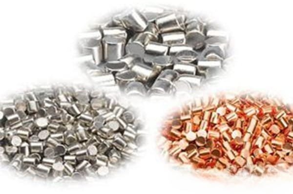
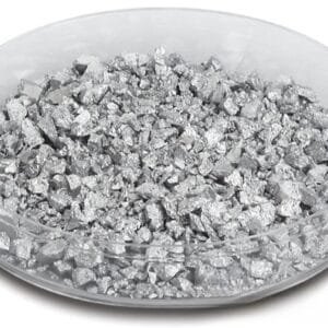
Our copper zinc evaporation materials, provided by Thin-Film Mat Engineering (TFM), are high-purity alloys consisting of copper (Cu) and zinc (Zn). These materials are essential for various deposition processes, ensuring the production of high-quality films. With purity levels up to 99.9995%, our copper zinc evaporation materials are manufactured under strict quality control standards to guarantee exceptional performance and reliability.

Applications of Copper Zinc Evaporation Materials

Copper zinc evaporation materials are utilized in a range of applications, including:

  • Deposition Techniques: Suitable for semiconductor deposition, chemical vapor deposition (CVD), and physical vapor deposition (PVD).
  • Optics: Used in wear-resistant coatings, decorative finishes, and display technologies.

Packaging and Handling

To preserve the quality of our copper zinc evaporation materials, we handle and package them with the utmost care. This careful handling ensures that the materials remain in pristine condition during storage and transportation.

Contact Us

Thin-Film Mat Engineering (TFM) is a leading provider of high-purity copper zinc evaporation materials and a variety of other evaporation products. We offer materials in both powder and granule forms, with customization options available upon request. For current pricing and information on additional deposition materials, please contact us directly.

Reviews

There are no reviews yet.

Be the first to review “VD0625 Copper Zinc Evaporation Materials, Cu/Zn”

Your email address will not be published. Required fields are marked *

FAQ

  • They are high‐purity substances (e.g. metals, alloys, or compounds) used in thermal or electron‐beam evaporation processes to form thin films on substrates.

  • Typically, they’re processed into a form (often ingots, pellets, or wires) that can be efficiently vaporized. Preparation emphasizes high purity and controlled composition to ensure film quality.

  • Thermal evaporation and electron-beam (e-beam) evaporation are the two main techniques, where material is heated (or bombarded with electrons) until it vaporizes and then condenses on the substrate.

  • Thermal evaporation heats the material directly (often using a resistive heater), while e-beam evaporation uses a focused electron beam to locally heat and vaporize the source material—each method offering different control and energy efficiency.

  • Key parameters include source temperature, vacuum level, deposition rate, substrate temperature, and the distance between the source and the substrate. These factors influence film uniformity, adhesion, and microstructure.

  • Evaporation generally produces high-purity films with excellent control over thickness, and it is especially suitable for materials with relatively low melting points or high vapor pressures.

  • Challenges include issues with step coverage (due to line-of-sight deposition), shadowing effects on complex topographies, and possible re-evaporation of material from the substrate if temperature isn’t properly controlled.

  • Common evaporation materials include noble metals (e.g., gold, silver), semiconductors (e.g., silicon, germanium), metal oxides, and organic compounds—each chosen for its specific optical, electrical, or mechanical properties.

  • Selection depends on desired film properties (conductivity, optical transparency, adhesion), compatibility with the evaporation process, and the final device application (semiconductor, optical coating, etc.).

  • Optimizing substrate temperature, deposition rate, and chamber vacuum are critical for ensuring that the film adheres well and forms the intended microstructure without defects.

  • Troubleshooting may involve checking the source material’s purity, ensuring stable source temperature, verifying the vacuum level, adjusting the substrate’s position or temperature, and monitoring deposition rate fluctuations.

While evaporation tends to yield very high purity films with excellent thickness control, it is limited by its line-of-sight nature. In contrast, sputtering can deposit films more uniformly on complex surfaces and is more versatile for a broader range of materials.


Shopping Cart
Scroll to Top