
Introduction
The Cryolite Sputtering Target (Na₃AlF₆) is a fluoride-based ceramic material primarily used for depositing fluoride thin films with low refractive index and high optical transparency. As an aluminum sodium fluoride compound, cryolite plays an important role in optical coating systems, especially where controlled light transmission, anti-reflective performance, and electrical insulation are required.
In thin film deposition processes, cryolite targets are selected for their chemical stability, wide band gap, and compatibility with multilayer optical stacks. They are particularly suitable for research laboratories and industrial production lines involved in precision optical components and specialized dielectric coatings.
Detailed Description
Cryolite (Na₃AlF₆) is a crystalline fluoride compound characterized by low optical absorption in the visible and infrared regions. When fabricated into sputtering targets, it is typically produced using high-purity raw materials followed by controlled sintering to achieve dense, homogeneous ceramic bodies.
Because fluoride ceramics are inherently brittle, manufacturing focuses on:
High density and low porosity to reduce particle generation
Uniform grain structure to maintain stable sputtering rate
Controlled impurity levels to preserve optical transparency
Optional bonding to copper backing plates for enhanced thermal management
Cryolite targets are generally used in RF magnetron sputtering systems due to their insulating nature. Proper power ramp-up and stable vacuum conditions are important to prevent thermal shock or cracking.
The deposited films typically exhibit:
Low refractive index (~1.34–1.36 at 550 nm)
High transparency across UV–visible–IR ranges
Good chemical resistance in dry environments
Excellent dielectric properties
These characteristics make cryolite an effective low-index material in multilayer interference coatings.
Applications
Cryolite Sputtering Targets are widely applied in:
Anti-reflective (AR) coatings
Optical interference filters
Laser mirror coatings
Infrared transmission coatings
Dielectric insulation layers
Multilayer optical stacks paired with high-index materials (e.g., TiO₂, Ta₂O₅)
Research and development of fluoride-based thin films
In precision optics, cryolite films are often alternated with high-refractive-index layers to form high-performance interference structures.
Technical Parameters
| Parameter | Typical Value / Range | Importance |
|---|---|---|
| Chemical Formula | Na₃AlF₆ | Defines fluoride optical characteristics |
| Purity | 99.9% – 99.99% | Ensures optical clarity and film consistency |
| Diameter | 25 – 200 mm (custom) | Matches sputtering cathode holders |
| Thickness | 3 – 6 mm | Influences lifetime and deposition rate |
| Density | ≥ 95% theoretical | Reduces particle contamination |
| Bonding | Copper backing plate (optional) | Improves heat dissipation |
Custom shapes and segmented targets can be provided for large-area coating systems.
Comparison with Related Fluoride Materials
| Material | Key Advantage | Typical Application |
|---|---|---|
| Cryolite (Na₃AlF₆) | Low refractive index, stable fluoride film | AR coatings & optical stacks |
| Magnesium Fluoride (MgF₂) | Excellent UV transparency | UV optics & AR coatings |
| Aluminum Fluoride (AlF₃) | Good chemical stability | Protective fluoride coatings |
| Calcium Fluoride (CaF₂) | High IR transmission | Infrared optical systems |
Compared to MgF₂, cryolite offers a slightly different refractive index profile and can be advantageous in multilayer optical design optimization.
FAQ
| Question | Answer |
|---|---|
| Is Cryolite an insulating material? | Yes, it is a dielectric ceramic and typically requires RF sputtering. |
| Can the target be bonded to a backing plate? | Yes, copper backing improves thermal stability during sputtering. |
| Is it suitable for DC sputtering? | Generally no, unless specialized conductive configurations are used. |
| What film properties can be expected? | Low refractive index, high transparency, and good dielectric behavior. |
| How should it be stored? | Store in a dry environment to prevent moisture interaction. |
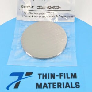
Packaging
Our Cryolite Sputtering Targets are meticulously tagged and labeled externally to ensure efficient identification and maintain high standards of quality control. We take great care to prevent any potential damage during storage and transportation, ensuring the targets arrive in perfect condition.
Conclusion
Cryolite Sputtering Targets provide a reliable low-index fluoride solution for advanced optical coatings and dielectric thin film applications. With controlled purity, stable sputtering behavior, and customizable dimensions, they are well suited for both research and industrial optical production environments.
For detailed specifications and a quotation, please contact us at sales@thinfilmmaterials.com.

Reviews
There are no reviews yet.