Introduction
Erbium Oxide (Er₂O₃) Sputtering Targets are advanced ceramic deposition materials widely used in thin film technologies, particularly in optical, semiconductor, and electronic applications. As a rare-earth oxide with excellent optical and dielectric properties, erbium oxide plays an important role in modern thin film engineering and photonic devices.
In Physical Vapor Deposition (PVD) processes such as RF magnetron sputtering, Er₂O₃ targets are used to produce high-purity erbium oxide thin films with precise composition and stable optical characteristics. These films are especially valued in optical coatings, laser systems, and semiconductor devices where rare-earth elements contribute unique electronic transitions and luminescence properties.
Detailed Description
Erbium Oxide Sputtering Targets are typically manufactured using high-purity erbium oxide powders through advanced ceramic processing techniques such as cold isostatic pressing (CIP), sintering, or hot pressing. These methods produce dense, uniform targets with excellent structural integrity and stable sputtering performance.
Er₂O₃ is a chemically stable rare-earth oxide with high melting temperature and excellent resistance to thermal and chemical degradation. These characteristics make it suitable for demanding thin film deposition processes that require long target lifetimes and consistent film quality.
During sputtering deposition, Er₂O₃ targets are usually operated using RF magnetron sputtering, which is preferred for insulating ceramic materials. The resulting thin films exhibit good optical transparency, dielectric strength, and luminescent properties. Erbium ions are particularly known for their optical emission around 1.55 μm, a wavelength widely used in optical communication systems.
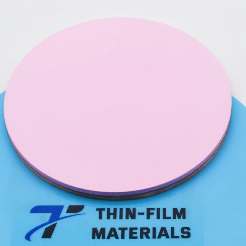
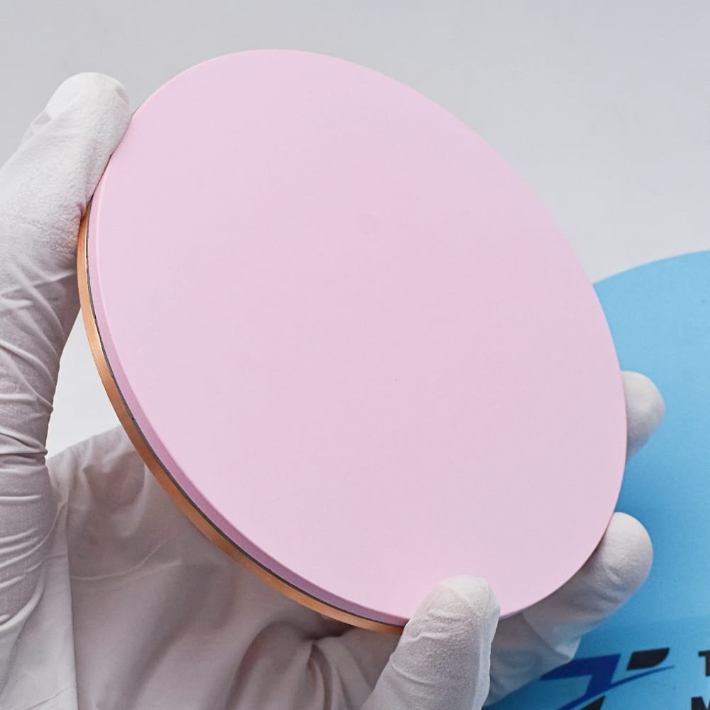
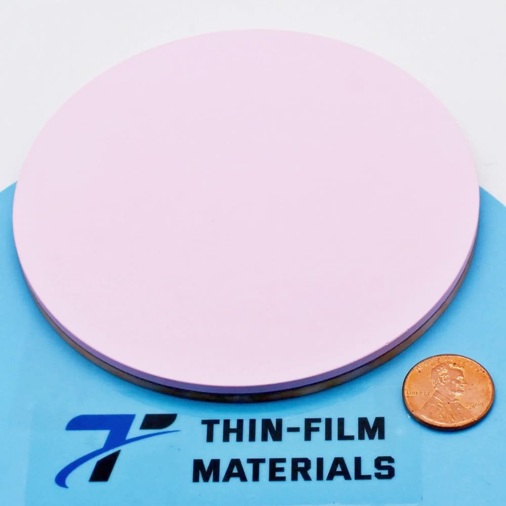
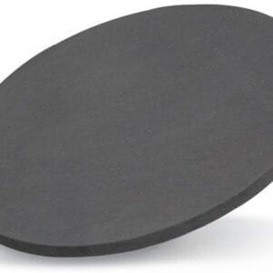
Er₂O₃ targets can be supplied in a variety of geometries including circular discs, rectangular plates, and custom shapes compatible with different sputtering systems. For larger targets or high-power sputtering systems, the material may be bonded to a copper backing plate using indium bonding or elastomer bonding to enhance heat dissipation and improve operational stability.
High-density erbium oxide targets minimize particle generation and arcing during deposition, ensuring smoother thin films and higher deposition efficiency in semiconductor and optical coating environments.
Applications
Thin films produced using Erbium Oxide Sputtering Targets are widely used across advanced technology sectors:
Optical coatings – used in infrared optical coatings and anti-reflective layers.
Optical communication devices – erbium-doped materials are essential for fiber amplifiers and photonic components.
Semiconductor thin films – used in dielectric layers and advanced microelectronic structures.
Laser and photonic materials – erbium ions provide strong luminescent properties useful in lasers and optical amplifiers.
Display and photonics research – used in functional optical thin films and luminescent coatings.
Protective coatings – erbium oxide layers offer chemical and thermal stability for specialized environments.
Technical Parameters
| Parameter | Typical Value / Range | Importance |
|---|---|---|
| Purity | 99.9% – 99.99% | Higher purity improves optical transparency and film performance |
| Density | ≥95% theoretical | Higher density improves sputtering stability and target lifetime |
| Diameter | 25 – 300 mm (custom) | Compatible with various sputtering systems |
| Thickness | 3 – 6 mm | Influences sputtering rate and film uniformity |
| Bonding | Copper / Titanium backing plate (optional) | Improves heat transfer and mechanical stability |
Comparison with Related Materials
| Material | Key Advantage | Typical Application |
|---|---|---|
| Erbium Oxide (Er₂O₃) | Strong infrared luminescence at 1.55 μm | Optical amplifiers and photonic devices |
| Yttrium Oxide (Y₂O₃) | Excellent dielectric properties | Protective and optical coatings |
| Lanthanum Oxide (La₂O₃) | High refractive index | Optical and electronic thin films |
FAQ
| Question | Answer |
|---|---|
| Can the Er₂O₃ sputtering target be customized? | Yes, diameter, thickness, purity, and bonding options can be customized based on deposition system requirements. |
| What sputtering method is recommended for Er₂O₃ targets? | RF magnetron sputtering is commonly used for ceramic oxide targets to maintain stable plasma conditions. |
| Are bonded targets available? | Yes, erbium oxide targets can be indium-bonded or elastomer-bonded to copper backing plates for better thermal management. |
| What substrates are commonly used with Er₂O₃ films? | Silicon wafers, quartz, sapphire, glass, and oxide substrates are commonly used depending on the application. |
| Which industries use erbium oxide sputtering targets most frequently? | Optical communications, semiconductor manufacturing, photonics research, and advanced optical coating industries. |
Packaging
Our Erbium Oxide Sputtering Targets are meticulously tagged and labeled externally to ensure efficient identification and maintain high standards of quality control. We take great care to prevent any potential damage during storage and transportation, ensuring the targets arrive in perfect condition.
Conclusion
The Erbium Oxide (Er₂O₃) Sputtering Target is an essential material for producing high-performance optical and electronic thin films. Its excellent optical properties, chemical stability, and compatibility with RF sputtering make it a reliable choice for applications in photonics, semiconductor devices, and optical coatings.
With customizable dimensions, high purity levels, and reliable bonding options, erbium oxide sputtering targets can meet the demanding requirements of both research laboratories and industrial thin film production.
For detailed specifications and a quotation, please contact us at sales@thinfilmmaterials.com.

Reviews
There are no reviews yet.