
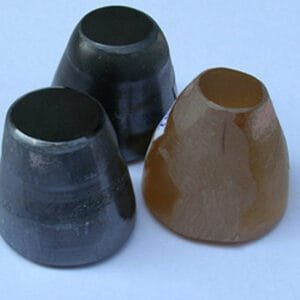
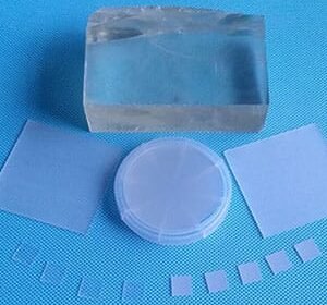
Gallium Antimonide Wafer (GaSb)
Gallium Antimonide (GaSb) is a crucial semiconductor material in the III-V element family. It plays an essential role in uncooled medium- to long-wave infrared detectors and focal plane arrays, offering high sensitivity, reliability, and a long operational life. GaSb wafers are widely used in infrared lasers, detectors, sensors, and thermal photovoltaic cells.
Gallium Antimonide Wafer Physical Properties
| Material | GaSb |
|---|---|
| Growth Method | LEC, VGF, VBG |
| Lattice (Å) | a = 6.094 |
| Structure | M3 |
| Melting Point | 712°C |
| Density (g/cm³) | 5.53 g/cm³ |
| Doped Materials | Undoped, Te-doped, Zn-doped |
| Type | P, P, N |
| Carrier Concentration (cm⁻³) | (1-2) x 10¹⁷, (5-100) x 10¹⁷, (1-20) x 10¹⁸ |
| Mobility (cm²/V·s) | 600-700, 200-500, 2000-350 |
| EPD (Average) | <2000/cm², <2000/cm², ≤2000/≤500/cm² |
Gallium Antimonide Wafer Specifications
| Size | 10mm x 10mm, 10mm x 5mm, 2″ Dia, 3″ Dia (custom sizes available) |
|---|---|
| Thickness | 500 µm, 600 µm, 800 µm (Tolerance: ±25 µm) |
| Polished | SSP or DSP |
| Orientation | <100>, <111> |
| Redirection Precision | ±0.5° |
| Primary Flat Length | 16±2 mm, 22±2 mm, 32.5±2 mm |
| Secondary Flat Length | 8±1 mm, 11±1 mm, 18±1 mm |
| TTV | <10 µm, <20 µm |
| Bow | <10 µm, <20 µm |
| Warp | <15 µm, <20 µm |
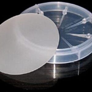
Gallium Antimonide Wafer Packaging
GaSb wafers are carefully packaged in a class 100 clean bag or wafer container within a class 1000 clean room to maintain optimal cleanliness and protect the wafers from contamination.
4o mini
Reviews
There are no reviews yet.