Generic selectors
Exact matches only
Search in title
Search in content
Post Type Selectors

ST0946 Gallium Arsenide Sputtering Target, GaAs

Chemical Formula GaAs
Catalog No. ST0946
CAS Number 1303-00-0
Purity 99.9%, 99.95%, 99.99%, 99.995%, 99.999%
Shape Discs, Plates, Column Targets, Step Targets, Custom-made

Gallium Arsenide sputtering target  come in various forms, purities, sizes, and prices. Thin Film Materials (TFM) manufactures and supplies top-quality sputtering targets at competitive prices.

MSDS File

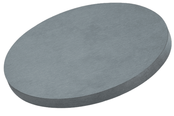
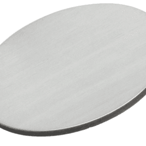
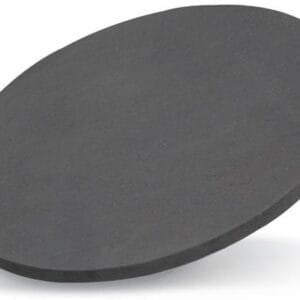
Gallium Arsenide Sputtering Target Description

Gallium Arsenide Sputtering Targets are utilized in the production of Gallium Arsenide (GaAs) films through thin film deposition techniques such as electron beam evaporation and magnetron sputtering. GaAs is a semiconductor material known for its exceptional properties, making it highly valuable in both electronics and optoelectronics.

Key characteristics of GaAs include:

  • Direct Energy Gap: GaAs has a direct bandgap, which is advantageous for optoelectronic applications. This makes it suitable for devices like photodetectors and lasers.
  • High Electron Mobility: The high electron mobility of GaAs is crucial for high-frequency and microwave applications.
  • Thermal Stability: GaAs maintains good thermal stability, allowing it to operate effectively in high-temperature environments.

Due to these properties, GaAs is ideal for a range of applications, including solar cells, photodetectors, laser diodes, and high-speed electronic devices. Its high electron saturation drift rate further enhances its performance in high-speed applications.

Related Product: Zinc Oxide with Gallium Oxide Sputtering Target, Gallium (III) Telluride Sputtering Target

Gallium Arsenide Sputtering Target Specifications

Compound Formula GaAs
Molecular Weight 144.64
Appearance Grey Target
Melting Point 1238 °C
Density 5.3 g/cm3
Available Sizes Dia.: 1.0″, 2.0″, 3.0″, 4.0″, 5.0″, 6.0″

Thick: 0.125″, 0.250″

Gallium Arsenide Sputtering Target Handling Notes

Indium bonding is recommended for Gallium Arsenide (GaAs) Sputtering Targets due to specific challenges associated with the material:

  • Brittleness: GaAs can be brittle, making it prone to cracking or breaking during the sputtering process.
  • Low Thermal Conductivity: GaAs has low thermal conductivity, which can lead to uneven temperature distribution and potential thermal stress during deposition.
  • Thermal Shock Susceptibility: The material’s susceptibility to thermal shock can cause instability during sputtering if not managed properly.

Indium bonding helps address these issues by providing better thermal and mechanical stability, ensuring that the GaAs Sputtering Targets perform optimally and maintain their integrity throughout the deposition process.

Gallium Arsenide Sputtering Target Application

Gallium Arsenide Sputtering Targets are versatile and valuable in several advanced applications:
  1. Semiconductor Device Preparation: Utilized in sputtering deposition techniques like Physical Vapor Deposition (PVD) and Chemical Vapor Deposition (CVD) to create thin films of GaAs for various semiconductor devices.
  2. Microwave and RF Devices: Employed in the production of high-performance microwave and RF devices, such as High Electron Mobility Transistors (HEMTs). The high electron mobility of GaAs is crucial for high-frequency and millimeter-wave applications, including communications equipment and radar systems.
  3. Magnetics Research: Used in research related to magnetic materials, particularly in studies exploring the magnetic properties of GaAs and its applications in magnetism.
  4. Semiconductor Nanostructure Preparation: Applied in the fabrication of semiconductor nanostructures, including nanowires and nanodots, for the development of innovative nanoelectronic devices.

These applications leverage the unique properties of GaAs, including its semiconducting nature, direct energy gap, and high electron mobility, to advance technology in electronics, optoelectronics, and beyond.

Gallium Arsenide Sputtering Target Packaging

Our Gallium Arsenide Sputtering Target is meticulously handled during storage and transportation to ensure that it retains its original quality and performance.

Get Contact

TFM offers Gallium Arsenide Sputtering Targets in various forms, purities, sizes, and prices. We specialize in high-purity thin film deposition materials with optimal density and minimal grain sizes, which are ideal for semiconductor, CVD, and PVD applications in display and optics. Contact Us for current pricing on sputtering targets and other deposition materials that are not listed.

Reviews

There are no reviews yet.

Be the first to review “ST0946 Gallium Arsenide Sputtering Target, GaAs”

Your email address will not be published. Required fields are marked *

Related Products

FAQ

It’s the source material (in solid form) used in sputter deposition to eject atoms or molecules that then form a thin film on a substrate.

Targets can be pure metals (e.g., gold, copper, aluminum), ceramics (e.g., Al₂O₃, SiO₂, TiO₂), alloys, or composites—chosen based on the film’s desired properties.


They are produced by processes such as melting/casting for metals or sintering (often with hot isostatic pressing) for ceramics and composite targets to ensure high density and purity.


In a vacuum chamber, a plasma (typically argon) bombards the target, ejecting atoms that travel and condense on a substrate, forming a thin film.


Key factors include the target’s purity, density, grain structure, and the sputtering yield (i.e. how many atoms are ejected per incident ion), as well as operating conditions like power density and gas pressure.


Operators monitor target erosion (often by measuring the depth of the eroded “race track”) or track total energy delivered (kilowatt-hours) until it reaches a threshold that can compromise film quality.


Fragile materials (such as many ceramics or certain oxides) and precious metals often require a backing plate to improve cooling, mechanical stability, and to allow thinner targets that reduce material costs.


DC sputtering is used for conductive targets, while RF sputtering is necessary for insulating targets (like many oxides) because it prevents charge buildup on the target’s surface.


In reactive sputtering, a reactive gas (e.g., oxygen or nitrogen) is introduced to form compound films on the substrate, but it may also “poison” the target surface if not carefully controlled.


Many manufacturers prefer to control raw material quality by sourcing their own powders; using external powders can risk impurities and inconsistent target properties.


Targets should be stored in clean, dry conditions (often in original packaging or re-wrapped in protective materials) and handled with gloves to avoid contamination, ensuring optimal performance during deposition.

Deposition rate depends on factors such as target material and composition, power density, working gas pressure, substrate distance, and the configuration of the sputtering system (e.g., magnetron design).

 
Shopping Cart
Scroll to Top