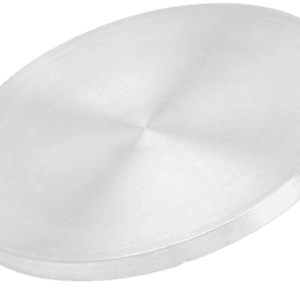
Gallium Nitride (GaN) Sputtering Target
The Gallium Nitride (GaN) sputtering target from Thin Film Materials (TFM) is a high-purity ceramic material engineered for demanding thin-film deposition processes in semiconductor, optoelectronic, and power device manufacturing. GaN is a wide-bandgap semiconductor known for its high breakdown voltage, excellent thermal stability, and outstanding electron mobility, making it essential for next-generation electronic and photonic components.
Product Overview
TFM supplies GaN sputtering targets with high density, fine-grain microstructure, and purities ranging from 99.9% (3N) to 99.99% (4N). These materials support stable sputtering behavior and deliver uniform, high-quality GaN thin films suitable for both R&D and industrial production.
Chemical Formula: GaN
Appearance: Black to dark gray ceramic
Density: ~6.15 g/cm³
Thermal Behavior: Decomposes before melting (~2,500 °C in air)
Crystal Structure: Wurtzite (hexagonal)
Standard geometries include round, rectangular, and step-type targets. Custom specifications and bonded configurations can be manufactured upon request. Indium or elastomer bonding onto copper or titanium backing plates is available to enhance thermal conductivity and target stability.
Applications
GaN sputtering targets are widely used in high-performance electronic and photonic devices, including:
Semiconductors: HEMTs, high-power switching components
Optoelectronics: LEDs, laser diodes, photodetectors
RF & Microwave Devices: 5G, radar, satellite communication modules
Energy Technologies: Thin-film photovoltaic and photoelectrochemical devices
Advanced Research: Quantum materials, wide-bandgap semiconductor studies
Technical Parameters
| Parameter | Typical Value / Range | Importance |
|---|---|---|
| Purity | 99.9% – 99.99% | Ensures high-quality films with minimal defects |
| Diameter | 25 – 150 mm (custom up to 300 mm) | Compatible with a wide range of sputtering tools |
| Thickness | 3 – 6 mm | Influences sputtering performance and lifetime |
| Bonding Options | Indium / Elastomer | Enhances heat transfer and durability |
| Backing Plate | Copper / Titanium | Provides mechanical support and thermal stability |
Comparison with Related Materials
| Material | Key Advantage | Typical Application |
|---|---|---|
| GaN | Wide bandgap, high electron mobility | Power devices, LEDs, RF components |
| SiC | Extreme thermal stability, hardness | Power electronics, protective coatings |
| ZnO | Transparency, low cost | Displays, general optoelectronics |
This comparison helps engineers select the optimal material for their specific deposition and device requirements.
Frequently Asked Questions
| Question | Answer |
|---|---|
| Can GaN sputtering targets be customized? | Yes. Custom diameters, thicknesses, purity levels, and bonded configurations are available. |
| Do you provide bonding services? | Yes. Indium and elastomer bonding for Cu or Ti backing plates can be supplied. |
| How are GaN sputtering targets packaged? | Vacuum-sealed, foam-protected, and shipped in export-safe cartons or wooden crates. |
| Which industries use GaN targets most? | Semiconductor, optoelectronics, power electronics, LED/laser manufacturing, and R&D institutions. |
| What purity levels are available? | 99%, 99.9%, and 99.99%, depending on application requirements. |
| What deposition methods are GaN targets used for? | Mainly RF magnetron sputtering and reactive sputtering. |
| Can the target shape be customized? | Yes. Round, rectangular, step-type, and other custom geometries are available. |
| What backing plate materials are recommended? | Copper, OFC, and titanium for superior heat dissipation and mechanical support. |
| How should GaN sputtering targets be stored? | Keep sealed, store in a dry and clean environment, avoid contamination. |
| What are the main applications of GaN films? | High-frequency, high-power, and optoelectronic thin-film devices. |
Packaging
All GaN sputtering targets are vacuum-sealed to prevent contamination and oxidation. Each item is secured with protective foam and delivered in export-approved cartons or wooden crates to ensure safe handling and transport.
Conclusion
The Gallium Nitride (GaN) sputtering target from TFM combines high purity, reliable performance, and flexible customization options to meet the requirements of advanced thin-film processes. With high-density ceramic fabrication, professional bonding services, and consistent sputtering stability, our GaN targets are suitable for both industrial production and cutting-edge research.
For detailed specifications, custom solutions, or a quotation, please contact sales@thinfilmmaterials.com.


Reviews
There are no reviews yet.