
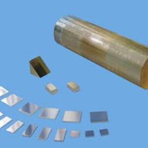
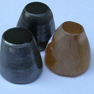
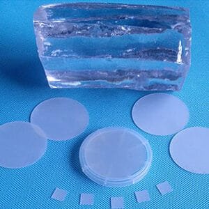
TFM’s Gallium Nitride Wafers: Precision and Performance Redefined
TFM takes pride in manufacturing premium-quality Gallium Nitride (GaN) wafers, built with advanced technological expertise and meticulous craftsmanship. As a recognized leader in the semiconductor materials industry, TFM is dedicated to providing reliable, high-precision solutions tailored to meet the evolving needs of our customers.
Our GaN wafers stand out for their unmatched consistency and superior manufacturing processes, setting a benchmark in the industry. With a commitment to continuous innovation, TFM remains at the cutting edge of wafer production, contributing to technological advancements with dependable, high-performance materials.
Gallium Nitride Wafer Specifications
| Specification | Details |
|---|---|
| Size | 10.0 mm x 10.5 mm, 14.0 x 15.0 mm, 2″ Dia, 4″ Dia |
| Thickness | 400 μm ± 30 μm / 450 μm ± 30 μm |
| Polished | Front Surface: Ra < 0.2 nm, Epi-ready polished Back Surface: Fine ground |
| Orientation | C-axis (0001) ± 0.5° |
| TTV | < 15 μm |
| Bow | < 20 μm |
Gallium Nitride Wafer Physical Properties
| Property | Details |
|---|---|
| Material | GaN |
| Conduction Type | N-Type |
| Resistivity (300K) | < 0.02 Ω·cm / < 0.2 Ω·cm / > 1E8 Ω·cm |
| EPD (Average) | Less than 5 x 10⁶ cm⁻² |
| Usable Surface Area | > 90% |
| Grade | Production, Research, Dummy |
Explore the exceptional performance and precision offered by TFM’s Gallium Nitride wafers, designed to empower next-generation semiconductor technologies.
Reviews
There are no reviews yet.