
 MSDS File
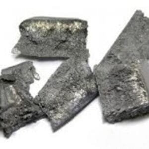
| Material Type | Gallium(III) Sulfide |
| Symbol | Ga2S3 |
| Color/Appearance | yellow |
| Melting Point (°C) | 1,090 |
| Theoretical Density (g/cc) | 3.77 |
| Z Ratio | – |
| E-Beam | – |
| Thermal Evaporation Techniques | Boat: – Crucible: – |
| E-Beam Crucible Liner Material | – |
| Temp. (°C) for Given Vap. Press. (Torr) | – |
| Comments | – |
Gallium(III) Sulfide Pellet Evaporation Material
TFM offers high-purity Gallium(III) Sulfide Pellet Evaporation Material, specifically designed for thin-film deposition in semiconductor, optoelectronic, and photonic applications. Composed of gallium (Ga) and sulfur (S), this material is used to create gallium sulfide (Ga2S3) thin films, which are important in applications requiring high optical transparency, electrical conductivity, and semiconducting properties. Gallium sulfide is a wide-bandgap semiconductor, making it suitable for infrared optoelectronics, photodetectors, and solar cells.
This material is engineered for thermal evaporation and electron beam (E-beam) evaporation, providing uniform film thickness, superior purity, and high adhesion to substrates, making it ideal for use in advanced thin-film applications.
Key Features and Advantages
Wide Bandgap Semiconductor: Gallium(III) Sulfide provides a wide bandgap, ideal for use in infrared optoelectronic devices, photodetectors, and solar energy applications.
High Optical Transparency: Features high optical transparency in the infrared spectrum, enhancing its suitability for optical communication systems and light-sensitive devices.
Excellent Electrical Properties: Offers good electrical conductivity while maintaining semiconductor characteristics, making it useful in optoelectronic devices.
High Purity & Uniform Deposition: Ensures precise deposition of high-quality films, reducing defects and improving device performance.
Customizable Composition: TFM’s Gallium(III) Sulfide material can be tailored to meet specific needs for advanced research and industrial applications.
Applications
Infrared Optoelectronics: Used in infrared sensors, photodetectors, and optical communication systems, ideal for applications in night vision, thermal imaging, and security systems.
Semiconductor Devices: Plays a key role in semiconductor technologies, such as transistors, photodetectors, and diodes.
Solar Cells: Contributes to the development of high-efficiency photovoltaic devices, improving light absorption and photoelectric conversion.
Thin-Film Coatings: Suitable for optical coatings in optoelectronics and photonic systems, offering high transparency and superior material stability.
High-Power Electronics: Supports high-power optoelectronic devices that require low loss and high efficiency.
Industry Impact and Customization
TFM’s Gallium(III) Sulfide Pellet Evaporation Material is essential for the development of infrared optoelectronics, semiconductor devices, and solar technologies. By providing customizable compositions, high purity, and precise deposition control, TFM ensures that its material solutions meet the requirements of advanced research and industrial applications.
With its wide-bandgap semiconductor properties, excellent optical transparency, and reliable performance, TFM’s Gallium(III) Sulfide Pellet Evaporation Material plays a significant role in the development of next-generation optoelectronic devices, photodetectors, and solar cells, ensuring high efficiency, long-term stability, and outstanding performance.


Reviews
There are no reviews yet.