
 MSDS File
Introduction
Germanium Nitride (Ge₃N₄) Evaporation Materials are advanced compound sources developed for high-performance thin film deposition in semiconductor, optoelectronic, and dielectric applications. As a germanium-based nitride, Ge₃N₄ offers promising electrical insulation characteristics, chemical stability, and compatibility with germanium-containing device architectures.
Ge₃N₄ evaporation materials are used in thermal and electron beam evaporation systems where controlled stoichiometry and high purity are required to produce uniform nitride thin films for next-generation electronic devices and research applications.
Detailed Description
Germanium Nitride is a covalently bonded compound formed between germanium and nitrogen, typically synthesized under controlled nitridation conditions to achieve phase purity and stable composition. Because nitrides are sensitive to oxygen contamination, strict control of raw materials and processing atmosphere is essential.
Ge₃N₄ evaporation materials are produced through:
Controlled chemical synthesis or solid-state reaction
Vacuum sintering or consolidation
Purification to minimize oxygen and metallic impurities
Maintaining the correct Ge:N ratio is critical, as deviations can influence dielectric strength, leakage current behavior, and film uniformity. During evaporation, careful control of temperature ramping and chamber pressure is required to preserve stoichiometry and avoid preferential decomposition.
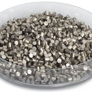
Available forms include:
Granules for resistive evaporation
Pressed pellets for stable evaporation rates
Custom-shaped pieces for electron beam crucibles
Deposited Ge₃N₄ thin films typically exhibit:
Good dielectric properties
Chemical stability in moderate environments
Compatibility with germanium-based semiconductor structures
Potential application as insulating or passivation layers
Due to its compound nature, e-beam evaporation is often preferred for improved compositional transfer and deposition control.
Applications
Germanium Nitride evaporation materials are used in:
Semiconductor Devices – Insulating or passivation layers
Germanium-Based Electronics – Integration with Ge substrates
Thin Film Transistors (TFTs) – Experimental dielectric layers
Optoelectronic Research – Functional nitride thin films
Advanced Materials Development – Nitride-based thin film engineering
Ge₃N₄ is primarily used in research and specialized semiconductor fabrication environments.
Technical Parameters
| Parameter | Typical Value / Range | Importance |
|---|---|---|
| Purity | 99.9% – 99.99% | Reduces defect density and improves dielectric performance |
| Chemical Formula | Ge₃N₄ | Ensures proper stoichiometry |
| Form | Granules / Pellets / Custom Pieces | Compatible with evaporation systems |
| Deposition Method | Thermal / E-beam Evaporation | Enables controlled thin film growth |
| Oxygen Content | Low ppm-level control | Prevents dielectric degradation |
| Phase Purity | Single-phase compound | Ensures consistent electrical behavior |
Comparison with Related Materials
| Material | Key Advantage | Typical Application |
|---|---|---|
| Ge₃N₄ | Compatible with Ge electronics | Semiconductor research |
| Si₃N₄ | Mature dielectric material | CMOS insulation |
| AlN | High thermal conductivity | Power electronics |
| GaN | Wide bandgap semiconductor | Optoelectronics |
Compared to Si₃N₄, Ge₃N₄ offers better structural compatibility with germanium-based devices, supporting advanced Ge integration strategies.
FAQ
| Question | Answer |
|---|---|
| Can Ge₃N₄ evaporation materials be customized? | Yes, purity level and physical form can be tailored for specific deposition systems. |
| Is e-beam evaporation recommended? | Yes, e-beam evaporation is often preferred for improved stoichiometric control. |
| Does Ge₃N₄ require special storage? | It should be stored in dry, controlled environments to prevent moisture contamination. |
| What industries use Ge₃N₄ most? | Semiconductor R&D, advanced electronics research, and materials science laboratories. |
| How is the material packaged? | Vacuum-sealed with moisture protection and export-grade cartons for safe transport. |
Packaging
Our Germanium Nitride Evaporation Materials are meticulously tagged and labeled externally to ensure efficient identification and maintain high standards of quality control. We take great care to prevent any potential damage during storage and transportation, ensuring the materials arrive in perfect condition.
Conclusion
Germanium Nitride (Ge₃N₄) Evaporation Materials provide a specialized solution for dielectric and semiconductor thin film deposition. With controlled stoichiometry, high purity, and customizable forms, Ge₃N₄ supports advanced germanium-based device development and nitride research applications.
For detailed specifications and a quotation, please contact us at sales@thinfilmmaterials.com.


Reviews
There are no reviews yet.