 MSDS File
Introduction
Germanium Selenide (GeSe₂) evaporation materials are widely used in thin-film deposition processes where precise optical, electronic, and infrared properties are required. As a chalcogenide compound semiconductor, GeSe₂ exhibits unique optical transparency in the infrared region and excellent glass-forming ability, making it highly valuable for advanced coatings and functional thin films. These characteristics make Germanium Selenide evaporation materials particularly important in research laboratories, semiconductor fabrication environments, and optical component manufacturing.
In physical vapor deposition (PVD) processes such as thermal evaporation or electron beam evaporation, GeSe₂ materials enable the formation of high-quality thin films with controlled stoichiometry and smooth morphology, supporting applications ranging from infrared optics to memory devices.
Detailed Description
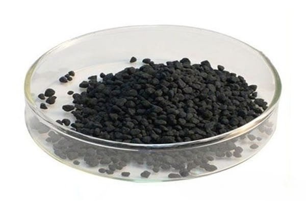
Germanium Selenide (GeSe₂) evaporation materials are typically supplied as high-purity granules, pieces, or pellets designed for stable and uniform evaporation during thin film deposition. The compound belongs to the family of chalcogenide materials known for their amorphous glass structures and tunable optical properties.
One of the most important attributes of GeSe₂ is its wide optical transparency in the infrared region, combined with relatively high refractive index and strong photo-sensitivity. These properties make it suitable for optical coatings and infrared photonic devices. When deposited as thin films, germanium selenide layers can exhibit excellent uniformity, high density, and strong adhesion to common substrates such as silicon, glass, or sapphire.
In vacuum evaporation systems, the purity and particle morphology of the evaporation material significantly influence the stability of the evaporation rate and the quality of the deposited films. High-purity GeSe₂ helps reduce contamination and defects, enabling the production of optically smooth films with consistent thickness. Additionally, controlled stoichiometry ensures that the deposited film maintains the desired optical bandgap and electrical behavior.
Germanium Selenide evaporation materials can also be tailored to specific deposition systems. Material forms, particle sizes, and packaging can be optimized for use in thermal evaporation boats, crucibles, or electron beam sources. These customization options help researchers and industrial users maintain stable deposition conditions and repeatable film properties.
Applications
Germanium Selenide evaporation materials are used across a variety of high-technology industries and research fields. Typical applications include:
Infrared optical coatings for lenses, sensors, and imaging systems
Chalcogenide glass thin films used in photonic and optoelectronic devices
Phase-change memory and electronic switching materials in semiconductor research
Waveguide and integrated photonic components
Infrared detectors and thermal imaging devices
Optical data storage and functional coatings
Because of its excellent infrared transparency and optical stability, GeSe₂ is particularly valuable in advanced photonics and IR optical systems.
Technical Parameters
| Parameter | Typical Value / Range | Importance |
|---|---|---|
| Purity | 99.9% – 99.999% | Higher purity reduces contamination in deposited films |
| Form | Granules / Pieces / Pellets | Ensures stable evaporation behavior |
| Particle Size | 1 – 6 mm (typical) | Influences evaporation rate and uniformity |
| Density | ~4.6 g/cm³ | Important for evaporation consistency |
| Melting Point | ~710 °C | Suitable for thermal and e-beam evaporation |
| Compatibility | Thermal / E-Beam Evaporation | Matches common PVD systems |
Comparison with Related Materials
| Material | Key Advantage | Typical Application |
|---|---|---|
| Germanium Selenide (GeSe₂) | High infrared transparency and optical stability | Infrared optics and photonics |
| Germanium Sulfide (GeS₂) | Wider bandgap and good glass formation | Optical coatings and glass systems |
| Selenium (Se) | Simple elemental material with high photosensitivity | Photoconductive films |
| Germanium (Ge) | High refractive index and semiconductor properties | Semiconductor and optical films |
FAQ
| Question | Answer |
|---|---|
| Can the GeSe₂ evaporation material be customized? | Yes, purity level, particle size, and packaging can be customized for specific deposition systems. |
| What deposition methods are compatible with GeSe₂? | Germanium Selenide can be used in thermal evaporation and electron beam evaporation systems. |
| How should GeSe₂ evaporation materials be stored? | They should be stored in sealed containers under dry conditions to avoid oxidation or contamination. |
| Which industries most commonly use GeSe₂ thin films? | Semiconductor research, infrared optics, photonics, and advanced electronic device development. |
| Is high purity important for GeSe₂ evaporation materials? | Yes, higher purity ensures better optical properties and minimizes defects in deposited thin films. |
Packaging
Our Germanium Selenide Evaporation Materials are meticulously tagged and labeled externally to ensure efficient identification and maintain high standards of quality control. We take great care to prevent any potential damage during storage and transportation, ensuring the targets arrive in perfect condition.
Conclusion
Germanium Selenide (GeSe₂) evaporation materials play a critical role in the fabrication of infrared optical coatings, photonic devices, and advanced semiconductor structures. Their excellent infrared transparency, stable evaporation characteristics, and compatibility with various deposition techniques make them an essential material in both research and industrial thin-film applications.
With customizable purity levels, particle sizes, and packaging options, these materials can be optimized to meet the specific requirements of modern thin film deposition systems.
For detailed specifications and a quotation, please contact us at sales@thinfilmmaterials.com.


Reviews
There are no reviews yet.