Germanium Sputtering Target
Introduction
Germanium Sputtering Target is a high-purity semiconductor material widely used in thin film deposition and optical coating applications. With excellent electrical properties, infrared transparency, and compatibility with various substrates, germanium is a vital material for producing infrared optics, semiconductor devices, and photovoltaic thin films. Its stable sputtering behavior ensures smooth film formation and consistent layer quality, making it an indispensable component in advanced coating systems.
Detailed Description
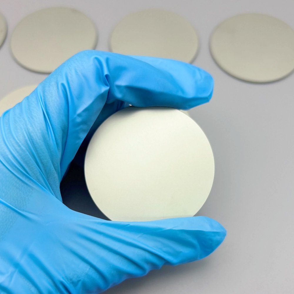
The Germanium Sputtering Target is made from refined germanium metal with a purity typically ranging from 99.99% (4N) to 99.999% (5N). It is processed through vacuum melting and precise machining to achieve uniform grain size, high density, and minimal oxygen contamination.
Key features include:
Excellent film uniformity: Enables precise control over thickness and optical properties.
High purity and density: Reduces impurities that could cause defects or irregularities in thin films.
Good thermal stability: Maintains consistent sputtering rate and adhesion under high-vacuum conditions.
Infrared transmission: Allows germanium-based coatings to be used in IR optical systems and detectors.
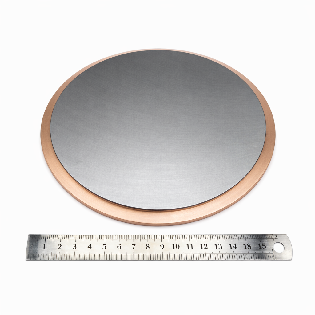
Customizable shapes and bonding options: Available as planar, rotary, and step targets with optional backing plates (copper or titanium) for better heat dissipation.
Applications
Germanium Sputtering Target serves in multiple industrial and research sectors, including:
Infrared optics: Production of IR lenses, windows, and detectors.
Semiconductor fabrication: Used in transistors, diodes, and integrated circuit layers.
Photovoltaic devices: As a key substrate or layer in thin-film solar cells.
Optical coatings: Anti-reflective and reflective coatings for optical instruments.
Research and development: Material studies and nanostructure coatings in universities and laboratories.
Technical Parameters
| Parameter | Typical Value / Range | Importance |
|---|---|---|
| Chemical Formula | Ge | Elemental composition |
| Purity | 99.99% – 99.999% | High purity ensures stable sputtering performance |
| Density | 5.323 g/cm³ | Influences film growth rate |
| Melting Point | 937.4 °C | Determines process temperature range |
| Electrical Resistivity | ~1.45 Ω·cm | Relevant for semiconductor applications |
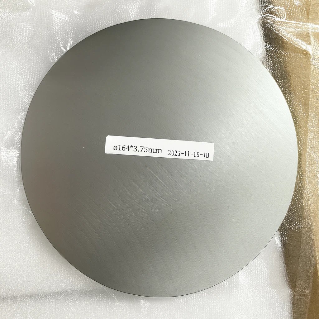
| Diameter | 25 – 300 mm (custom) | Fits different sputtering systems |
| Thickness | 3 – 6 mm | Affects sputtering rate and film uniformity |
| Backing Plate | Copper / Titanium | Improves heat dissipation and bonding strength |
Comparison with Related Materials
| Material | Key Advantage | Typical Application |
|---|---|---|
| Germanium (Ge) | Infrared transparency, semiconductor use | Optical coatings, solar cells |
| Silicon (Si) | Lower cost, widespread use | Microelectronics, semiconductor layers |
| Gallium Arsenide (GaAs) | Direct bandgap for optoelectronics | Lasers, LEDs, high-speed electronics |
FAQ
| Question | Answer |
|---|---|
| Can the target size be customized? | Yes. We provide custom diameters, thicknesses, and bonding types according to your system specifications. |
| What purity levels are available? | 4N (99.99%) and 5N (99.999%) are standard. Higher purities can be offered upon request. |
| Which sputtering systems are compatible? | Compatible with DC, RF, and magnetron sputtering systems. |
| How is it packaged? | Each target is vacuum-sealed with moisture protection and cushioned in export-safe wooden crates. |
| What industries commonly use germanium targets? | Semiconductor, optics, defense, aerospace, and energy research. |
| Is bonding recommended for large targets? | Yes. Copper or titanium backing is suggested for improved heat conduction and structural support. |
Packaging
Our Germanium Sputtering Targets are carefully packaged under inert atmosphere and vacuum-sealed to prevent oxidation. Each piece is labeled with purity, batch number, and dimensions for traceability. Protective foam and shockproof export cartons ensure safe delivery worldwide.
Conclusion
Germanium Sputtering Target offers an excellent combination of semiconductor functionality, optical clarity, and stability for advanced thin film deposition. Its high purity, consistent microstructure, and reliable sputtering behavior make it the preferred choice for both research and industrial coating applications.
For detailed specifications and quotations, please contact us at [sales@thinfilmmaterials.com].


Reviews
There are no reviews yet.