
Product Overview
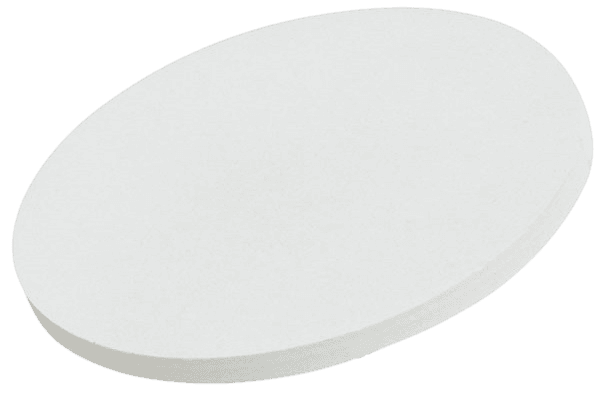
Indium Arsenide Sputtering Target (InAs) is a compound sputtering target used to deposit thin films where a specific pre-compounded chemistry is required. These materials can behave differently from conductive metallic targets in terms of electrical response, thermal shock resistance, density sensitivity, and cracking risk, so target dimensions, density, backing design, and sputtering mode should be considered together.
Material and Deposition Characteristics
The appropriate sputtering mode depends on target conductivity, thermal behavior, and the power-supply configuration. Many compound ceramic targets are evaluated first with RF magnetron sputtering, especially when electrical resistivity is high. For brittle or low-thermal-conductivity materials, density, backing support, and stable cooling are important for reliable operation.
Technical Data
| Parameter | Typical Value / Range | Importance |
|---|---|---|
| Chemical Composition | InAs | Determines bandgap and carrier mobility |
| Purity | 99.9% – 99.99% | Reduces defect density in thin films |
| Diameter | 25 – 200 mm (custom available) | Compatible with standard sputtering systems |
| Thickness | 3 – 6 mm | Influences target lifetime and sputtering rate |
| Density | ≥ 95% theoretical | Improves plasma stability |
| Sputtering Mode | RF sputtering | Suitable for semiconducting compounds |
| Bonding | Unbonded / bonded on request | Enhances thermal stability |
| Material | Key Advantage | Typical Application |
|---|---|---|
| InAs | Very high electron mobility, narrow bandgap | IR detectors & high-speed electronics |
| Indium Phosphide (InP) | Better thermal stability | Optoelectronics |
| Gallium Arsenide (GaAs) | Mature processing technology | RF & optoelectronic devices |
| Indium Antimonide (InSb) | Extremely narrow bandgap | Long-wavelength IR detection |
| Question | Answer |
|---|---|
| Can the InAs sputtering target be customized? | Yes, diameter, thickness, purity, and bonding options can be tailored. |
| Is RF sputtering required for InAs? | RF sputtering is commonly used due to the semiconducting nature of InAs. |
| How is the target packaged? | Vacuum-sealed with protective cushioning and export-grade cartons or crates. |
| Is InAs suitable for infrared applications? | Yes, InAs is widely used for IR-sensitive thin film devices. |
Typical Thin-Film Applications
- Compound thin films for semiconductor, optical, protective, hard-coating, and functional-material research
- Applications where a pre-compounded target is preferred over co-sputtering separate elemental targets
- Projects requiring controlled chemistry and tailored target geometry for PVD development
Target Configuration and Ordering Considerations
When requesting a quotation, provide target diameter or rectangular dimensions, thickness, purity or composition, required quantity, and whether a backing plate or bonded assembly is needed. For brittle ceramic or compound targets, it is useful to specify the cathode model, backing-plate material, preferred bonding method, operating power if known, and any density, tolerance, or inspection-document requirements. TFM can review drawings, old-target photos, and application details when custom dimensions are required.
Frequently Asked Questions
What is the main reason to use a Indium Arsenide sputtering target?
It provides a composition-specific source for depositing thin films when the required chemistry is better introduced from a pre-compounded target than from co-sputtering separate elements.
How should the sputtering mode for Indium Arsenide be selected?
The power mode should be selected from target conductivity, thermal behavior, and equipment capability. Many compound ceramic targets are first evaluated with RF magnetron sputtering.
Why are density and microstructure important for Indium Arsenide targets?
Uniform density and microstructure help support stable erosion and thermal behavior, while pores or local defects can increase the risk of cracking, particles, or unstable plasma.
Can a Indium Arsenide target be supplied with a backing plate?
Yes. Where the material is brittle or the cathode requires a backing assembly, bonded configurations can be reviewed according to target size, thickness, cooling, and operating power.
Does target composition always equal film composition?
No. Film chemistry can shift because of different sputtering yields, reactive conditions, substrate temperature, re-sputtering, or chamber history. Verify the film when the chemistry is critical.
What should I provide to request a quotation for Indium Arsenide?
Please provide material composition, purity, dimensions, quantity, target or backing configuration, cathode model or system details, and any drawing, tolerance, or inspection requirements.


Reviews
There are no reviews yet.