
Introduction
Indium Arsenide (InAs) wafers are a critical III–V compound semiconductor material widely used in advanced electronics and optoelectronics. Known for its exceptionally high electron mobility and narrow bandgap, InAs enables high-speed, low-noise, and infrared-sensitive devices that are difficult to achieve with conventional silicon-based materials. These wafers are essential substrates for cutting-edge research, prototype development, and specialized industrial applications.
Detailed Description
Indium Arsenide is a direct bandgap semiconductor with a bandgap of approximately 0.36 eV at room temperature. This narrow bandgap allows InAs wafers to respond efficiently to mid-infrared radiation, making them particularly valuable in infrared detection and sensing technologies.
One of the most significant advantages of InAs is its extremely high electron mobility, which supports ultrafast carrier transport. Devices fabricated on InAs wafers can operate at higher frequencies with reduced power loss, an important requirement for high-frequency electronics and low-temperature physics research.
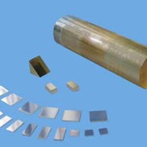
Our Indium Arsenide wafers are manufactured using controlled crystal growth processes to ensure uniform crystallographic orientation, low defect density, and consistent electrical properties. Wafers are available in common orientations such as (100) and (111), with single-side or double-side polishing options depending on device requirements. Surface quality, thickness uniformity, and flatness are carefully controlled to meet epitaxial growth and microfabrication standards.
Customization is available for diameter, thickness, orientation, doping type (n-type or undoped), and surface finish, allowing researchers and engineers to integrate InAs wafers seamlessly into Molecular Beam Epitaxy (MBE), Metal-Organic Chemical Vapor Deposition (MOCVD), or device fabrication workflows.
Applications
Indium Arsenide wafers are widely used across both research and specialized industrial fields, including:
Infrared detectors and focal plane arrays (FPAs) for thermal imaging and spectroscopy
High-electron-mobility transistors (HEMTs) and ultrafast electronic devices
Terahertz and millimeter-wave electronics
Quantum devices and low-temperature physics research
Epitaxial growth substrates for advanced III–V heterostructures
Magnetic sensors and Hall-effect devices requiring high sensitivity
Technical Parameters
| Parameter | Typical Value / Range | Importance |
|---|---|---|
| Material | Indium Arsenide (InAs) | Determines electronic and optical behavior |
| Crystal Structure | Zinc blende | Ensures predictable band structure |
| Orientation | (100), (111) | Influences epitaxial growth quality |
| Diameter | 2″ – 4″ (custom available) | Compatible with standard processing tools |
| Thickness | 350 – 625 µm | Affects mechanical strength and handling |
| Surface Finish | SSP / DSP | Impacts lithography and epitaxy results |
| Doping | Undoped / n-type | Controls electrical characteristics |
Comparison with Related Materials
| Material | Key Advantage | Typical Application |
|---|---|---|
| Indium Arsenide (InAs) | Extremely high electron mobility, IR sensitivity | High-speed electronics, IR detectors |
| Indium Phosphide (InP) | Good balance of speed and stability | Photonics, telecom |
| Gallium Arsenide (GaAs) | Mature processing, good RF performance | RF devices, LEDs |
| Silicon (Si) | Low cost, scalable | Mainstream electronics |
FAQ
| Question | Answer |
|---|---|
| Can InAs wafers be customized? | Yes, diameter, thickness, orientation, doping, and polishing can be tailored. |
| Are these wafers suitable for epitaxial growth? | Yes, they are compatible with MBE and MOCVD processes. |
| How are the wafers packaged? | Cleanroom-packed, vacuum-sealed, and shock-protected for safe transport. |
| What industries typically use InAs wafers? | Infrared imaging, quantum research, defense, aerospace, and advanced R&D. |
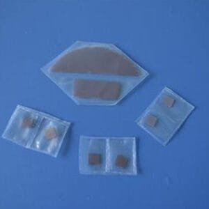
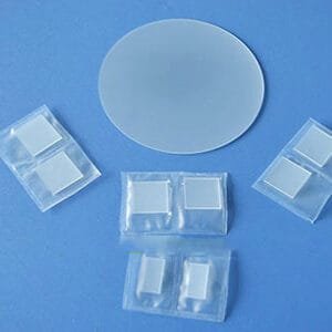
Packaging
Our Indium Arsenide Wafer (InAs) products are carefully labeled for full traceability and quality control. Each wafer is individually protected to prevent surface damage and contamination during storage and transportation. Export-grade packaging ensures the wafers arrive in pristine condition, ready for immediate use.
Conclusion
Indium Arsenide wafers offer unmatched performance for high-speed electronics and infrared-sensitive applications. With precise manufacturing control, reliable material quality, and flexible customization options, these wafers are an ideal choice for advanced research and specialized device fabrication.
For detailed specifications and a quotation, please contact us at sales@thinfilmmaterials.com.
Reviews
There are no reviews yet.