Generic selectors
Exact matches only
Search in title
Search in content
Post Type Selectors

Indium Phosphide Wafer (InP)

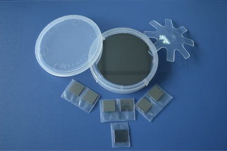
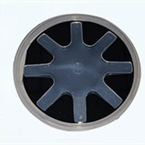
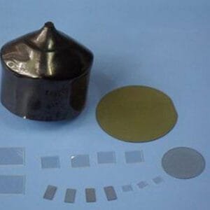
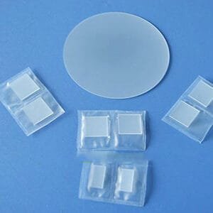
TFM Indium Phosphide Wafer: High Performance, High Precision

TFM provides high-purity Indium Phosphide Wafer (InP), renowned for their exceptional electronic and optoelectronic properties. InP wafers offer high electron mobility, direct bandgap characteristics, and superior thermal conductivity, making them ideal for high-speed, high-frequency, and photonic applications.

InP wafers are extensively used in optoelectronics, fiber-optic communication, and high-frequency RF devices, including laser diodes, photodetectors, and high-speed transistors. Their low lattice mismatch with III-V compound semiconductors ensures excellent epitaxial layer growth, enhancing device performance and efficiency.

TFM supplies InP wafers in various sizes and specifications, tailored to meet the stringent demands of semiconductor research and advanced device fabrication, ensuring optimal performance for next-generation electronic and optical technologies.

Indium Phosphide Wafer Specifications

Size10 x 10 x 0.35mm, 10 x 5 x 0.35mm, 2″ Dia, 3″ Dia, 4″ Dia (custom sizes available)
Thickness0.35 mm, 0.6 mm
PolishedSSP or DSP
Orientation<100>, <111>
Redirection Precision±0.5°
Primary Flat Length16±2 mm, 22±2 mm, 32.5±2 mm
Secondary Flat Length8±1 mm, 11±1 mm, 18±1 mm
TTV<10 µm, <15 µm
Bow<10 µm, <15 µm
Warp<15 µm

Indium Phosphide Wafer Physical Properties

MaterialInP
Growth MethodLEC, VCZ/P-LEC, VGF, VB
Lattice (Å)a = 5.869
StructureM3
Melting Point1600°C
Density (g/cm³)4.79 g/cm³
Doped MaterialsUndoped, S-doped, Zn-doped, Fe-doped
TypeN, N, P, N
Carrier Concentration (cm⁻³)(0.4-2) x 10¹⁶, (0.8-3) x 10¹⁸, (4-6) x 10¹⁸, (0.6-2) x 10¹⁸, 10⁷-10⁸
Mobility (cm²/V·s)(3.5-4) x 10³, (2.2-2.4) x 10³, (1.3-1.6) x 10³, 70-90, ≥2000
EPD (Average)<5 x 10⁴/cm², 3 x 10⁴/cm², 2 x 10³/cm², 2 x 10⁴/cm², 3 x 10⁴/cm²

Reviews

There are no reviews yet.

Be the first to review “Indium Phosphide Wafer (InP)”

Your email address will not be published. Required fields are marked *

FAQ

A thin film substrate is the base material upon which thin layers of materials are deposited to create electronic, optical, or mechanical devices. The substrate provides structural support and can influence the properties of the thin film.

The choice of substrate affects the film’s structural integrity, electrical properties, and overall performance. Factors like thermal expansion coefficient, surface smoothness, and chemical compatibility are crucial considerations.

Materials such as lanthanum aluminate (LaAlO₃), magnesium oxide (MgO), and strontium titanate (SrTiO₃) are commonly used due to their lattice compatibility and thermal stability, which are essential for optimal superconducting properties.

Metal substrates offer high electrical and thermal conductivity, making them suitable for applications requiring efficient heat dissipation and electrical connectivity. However, their surface properties and potential for oxidation must be managed during deposition.

These substrates are materials that can support the growth of thin films exhibiting magnetic or ferroelectric properties, essential for applications in memory devices, sensors, and actuators.

Semiconductor substrates, such as silicon wafers, serve as the foundation for integrated circuits and various electronic components, providing the necessary electrical characteristics and structural support for device fabrication.

Gallium Nitride (GaN) substrates are pivotal for high-performance optoelectronic and power devices due to their excellent thermal conductivity, high breakdown voltage, and efficiency. They are widely used in LEDs, power transistors, and RF components.

Halide crystal substrates, composed of halide compounds, are utilized in specialized optical applications, including infrared spectroscopy and laser systems, due to their unique optical properties.
Ceramic substrates provide high thermal stability, mechanical strength, and electrical insulation, making them ideal for high-frequency and high-power applications.
Proper surface preparation, including cleaning and polishing, ensures the removal of contaminants and surface irregularities, leading to improved film adhesion, uniformity, and performance.
Yes, thin films can be deposited on flexible substrates like polymers, enabling the development of flexible electronics and wearable devices. However, challenges include managing mechanical stress and ensuring film adhesion.
Challenges include ensuring lattice matching to minimize defects, managing thermal expansion differences to prevent stress and delamination, and achieving desired electrical and optical properties for specific applications.
Shopping Cart
Scroll to Top