
Iron Antimonide Sputtering Target (FeSb₂)
Introduction
Iron Antimonide (FeSb₂) Sputtering Target is a thermoelectric and semiconductor material widely used in thin film deposition for research and industrial applications. Its narrow bandgap and excellent Seebeck coefficient make it a promising compound for energy conversion devices, infrared detectors, and advanced electronic components. The FeSb₂ sputtering target enables precise thin film fabrication for studying correlated electron systems and thermoelectric phenomena.
Detailed Description
FeSb₂ is an intermetallic compound composed of iron (Fe) and antimony (Sb) in a 1:2 atomic ratio. This material exhibits a unique combination of semiconducting and metallic properties depending on temperature, making it of great interest for both physics research and device manufacturing.
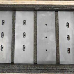
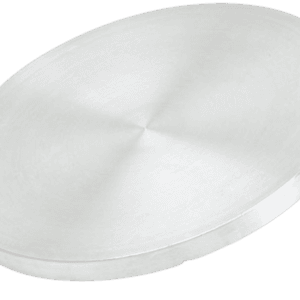
The Iron Antimonide Sputtering Target is typically manufactured using vacuum hot pressing or hot isostatic pressing (HIP) to achieve high density and excellent mechanical integrity. The resulting targets have a homogeneous microstructure, ensuring uniform thin film deposition during DC or RF magnetron sputtering.
Typical characteristics include:
High purity (99.9%–99.99%), minimizing contamination during sputtering.
Fine-grained, dense microstructure, which enhances sputtering efficiency and film uniformity.
Good thermal stability, ensuring consistent performance under prolonged sputtering conditions.
FeSb₂ thin films are often explored for thermoelectric applications because of their exceptional power factor and low thermal conductivity, making this target ideal for both research and pilot-scale production.
Applications
Iron Antimonide (FeSb₂) Sputtering Targets are commonly used in:
Thermoelectric thin films for energy harvesting and Peltier cooling devices.
Infrared and optical sensors, benefiting from the material’s narrow bandgap properties.
Semiconductor and spintronic devices for electronic material research.
Correlated electron and low-temperature physics studies, due to its unique electron transport behavior.
Functional coatings in advanced microelectronic and optoelectronic applications.
Technical Parameters
| Parameter | Typical Value / Range | Importance |
|---|---|---|
| Purity | 99.9% – 99.99% | High purity reduces impurities in deposited films |
| Composition | FeSb₂ (1:2 atomic ratio) | Ensures stoichiometric thin films |
| Density | 6.9 – 7.2 g/cm³ | Affects film growth rate and surface morphology |
| Diameter | 25 – 300 mm (custom) | Compatible with various sputtering systems |
| Thickness | 3 – 6 mm | Optimized for stable sputtering performance |
| Bonding | Indium / Copper backing | Improves heat dissipation and film uniformity |
Comparison with Related Materials
| Material | Key Advantage | Typical Application |
|---|---|---|
| FeSb₂ | High Seebeck coefficient, narrow-gap semiconductor | Thermoelectric & IR detectors |
| Bi₂Te₃ | Excellent thermoelectric performance at room temperature | Cooling modules |
| Sb₂Te₃ | Phase-change memory material | Data storage thin films |
FAQ
| Question | Answer |
|---|---|
| Can FeSb₂ targets be customized in size and bonding? | Yes, we can supply FeSb₂ targets in various diameters, thicknesses, and with or without backing plates such as copper or titanium. |
| What sputtering method is recommended? | Both DC and RF magnetron sputtering are suitable, depending on the substrate and desired film properties. |
| Is FeSb₂ brittle? | Yes, as an intermetallic compound, FeSb₂ is relatively brittle, so careful handling and mounting are recommended. |
| What are typical substrate materials? | Common substrates include Si, sapphire (Al₂O₃), and glass for thermoelectric or optical film growth. |
| Can FeSb₂ be used for thermoelectric applications? | Absolutely. FeSb₂ is known for its high thermoelectric power factor, making it valuable for energy conversion research. |
Packaging
Our FeSb₂ Sputtering Targets are carefully vacuum-sealed with protective foam and placed in export-grade cartons or wooden crates. Each piece is externally labeled for clear identification and traceability, ensuring safe transportation and perfect condition upon delivery.
Conclusion
The Iron Antimonide (FeSb₂) Sputtering Target offers researchers and engineers a reliable material for high-performance thermoelectric and semiconductor thin films. With its controllable stoichiometry, excellent purity, and compatibility with diverse sputtering systems, it supports both scientific discovery and industrial innovation.
For detailed specifications and a quotation, please contact us at [sales@thinfilmmaterials.com].

Reviews
There are no reviews yet.