
Product Overview
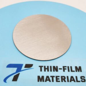
Lead Sulfide Sputtering Target (PbS) is a chalcogenide sputtering target intended for composition-sensitive thin-film deposition. For sulfur-, selenium-, or tellurium-containing materials, the target chemistry is only the starting point: sputtering yield differences, substrate temperature, gas pressure, and volatile-component loss can shift the deposited-film composition relative to the nominal target composition.
Material and Deposition Characteristics
These targets are commonly treated as mechanically brittle and composition-sensitive sputtering materials. RF sputtering is often considered when target conductivity is limited. Power density, substrate temperature, and working pressure should be controlled conservatively, and the deposited film composition should be verified when precise sulfur, selenium, or tellurium stoichiometry is required.
Technical Data
| Parameter | Typical Value / Range | Importance |
|---|---|---|
| Purity | 99.9% – 99.99% | High purity ensures stable semiconductor performance |
| Chemical Formula | PbS | Determines semiconductor structure and optical properties |
| Diameter | 25 – 300 mm (custom) | Compatible with common sputtering systems |
| Thickness | 3 – 6 mm | Influences sputtering rate and target lifetime |
| Density | ≥ 95% theoretical density | Ensures stable sputtering and uniform thin films |
| Bonding | Copper backing plate / Indium bonded | Improves thermal conductivity and target stability |
| Material | Key Advantage | Typical Application |
|---|---|---|
| Lead Sulfide (PbS) | Strong infrared absorption and narrow bandgap | Infrared detectors and optoelectronic films |
| Lead Selenide (PbSe) | Sensitive to longer infrared wavelengths | Thermal imaging and IR detectors |
| Cadmium Telluride (CdTe) | Excellent photovoltaic properties | Solar cells and radiation detectors |
| Question | Answer |
|---|---|
| What sputtering methods can be used with PbS targets? | PbS sputtering targets are typically used in RF magnetron sputtering systems suitable for compound semiconductors. |
| Can the PbS target size be customized? | Yes. Diameter, thickness, and bonding configurations can be customized to match specific sputtering equipment. |
| What purity levels are typically available? | Standard purities range from 99.9% to 99.99%, depending on application requirements. |
| Are bonded sputtering targets available? | Yes. Copper backing plates with indium bonding are commonly used to improve heat dissipation during deposition. |
| What substrates can PbS thin films be deposited on? | PbS films can be deposited on silicon wafers, glass, ceramics, and other semiconductor substrates. |
Typical Thin-Film Applications
- Chalcogenide thin films for optical, infrared, electronic, thermoelectric, and phase-change research
- Compound semiconductor layers and advanced-material thin-film studies
- Projects where composition retention and controlled sputtering of brittle materials are important
Target Configuration and Ordering Considerations
When requesting a quotation, provide target diameter or rectangular dimensions, thickness, purity or composition, required quantity, and whether a backing plate or bonded assembly is needed. For brittle ceramic or compound targets, it is useful to specify the cathode model, backing-plate material, preferred bonding method, operating power if known, and any density, tolerance, or inspection-document requirements. TFM can review drawings, old-target photos, and application details when custom dimensions are required.
Frequently Asked Questions
What sputtering mode is commonly used for Lead Sulfide?
RF magnetron sputtering is often considered when the target conductivity is limited or when more conservative operation is preferred for brittle, composition-sensitive compounds.
Can Lead Sulfide films lose sulfur, selenium, or tellurium during deposition?
Yes. Composition drift can occur because of preferential sputtering, substrate heating, re-sputtering, and volatile-component loss. Film composition should be checked when stoichiometry is important.
Why is bonding important for a Lead Sulfide target?
Many chalcogenide targets are brittle and have modest thermal conductivity. A suitable backing plate and bonding layer can improve mechanical support and heat transfer during sputtering.
Does the target composition guarantee film stoichiometry for PbS?
No. The target composition is the starting source composition, but the deposited film can still shift because of process variables. Film analysis should be used to confirm the final stoichiometry.
What process variables should be monitored when sputtering Lead Sulfide?
Useful variables include power density, working pressure, substrate temperature, cooling, target conditioning, and deposited-film composition. If reactive gas is used, gas ratio should also be controlled carefully.
What should I send TFM for a custom Lead Sulfide target?
Please provide composition or formula, purity, dimensions, quantity, backing or bonding details, cathode model, and any film-composition or inspection requirements relevant to your project.

Reviews
There are no reviews yet.