 MSDS File
Introduction
Lead(II) Titanate Evaporation Materials (PbTiO₃) are advanced perovskite oxide compounds used in the fabrication of ferroelectric and piezoelectric thin films. As a well-known ferroelectric material with a high Curie temperature (~490°C), PbTiO₃ is widely applied in non-volatile memory research, microelectromechanical systems (MEMS), sensors, and actuator technologies.
In vacuum deposition systems, PbTiO₃ evaporation materials enable the formation of functional oxide layers with strong spontaneous polarization and dielectric performance. Careful control of composition and oxygen environment is essential to maintain film stoichiometry and phase purity.
Detailed Description
PbTiO₃ is a tetragonal perovskite structured oxide composed of lead (Pb) and titanium (Ti) in a 1:1 atomic ratio. Due to the relatively high vapor pressure of lead at elevated temperatures, precise material preparation and deposition control are critical to avoid lead deficiency during evaporation.
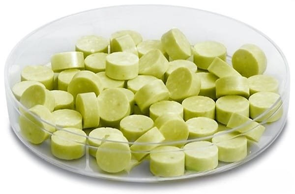
Evaporation materials are typically supplied as:
Sintered ceramic pellets
Granules
Pressed tablets
Custom-cut pieces compatible with crucibles
Manufacturing emphasizes:
High phase purity to avoid secondary phases (e.g., PbO segregation)
Controlled density (≥95% theoretical)
Homogeneous microstructure for stable evaporation
Optimized stoichiometry compensation if required
PbTiO₃ evaporation materials are generally used in electron beam evaporation systems, often under controlled oxygen partial pressure to maintain proper oxidation states. In some processes, co-evaporation with excess PbO is applied to compensate for lead volatility.
Deposited PbTiO₃ thin films typically exhibit:
Strong ferroelectric polarization
High dielectric constant
Good piezoelectric response
Structural compatibility with perovskite substrates
These properties make PbTiO₃ a foundational material in ferroelectric device engineering.
Applications
Lead(II) Titanate Evaporation Materials are widely used in:
Ferroelectric memory devices (FeRAM research)
Piezoelectric thin film actuators
MEMS sensors and micro-actuators
Perovskite oxide heterostructures
Capacitor and dielectric layer research
Spintronic and multiferroic material development
Academic and advanced R&D laboratories
PbTiO₃ is often integrated with related perovskite materials such as PZT (lead zirconate titanate) systems for enhanced electromechanical performance.
Technical Parameters
| Parameter | Typical Value / Range | Importance |
|---|---|---|
| Chemical Formula | PbTiO₃ | Defines ferroelectric perovskite structure |
| Purity | 99.9% – 99.99% | Ensures phase stability & electrical performance |
| Form | Pellets / Granules / Pieces | Compatible with evaporation sources |
| Density | ≥ 95% theoretical | Improves evaporation consistency |
| Deposition Method | E-beam (with O₂ control) | Maintains stoichiometry |
| Curie Temperature | ~490°C | Defines ferroelectric operating range |
Custom pellet sizes and stoichiometry adjustments can be provided for specific research requirements.
Comparison with Related Ferroelectric Materials
| Material | Key Advantage | Typical Application |
|---|---|---|
| PbTiO₃ | High Curie temperature & strong polarization | Ferroelectric thin films |
| PZT (Pb(Zr,Ti)O₃) | Enhanced piezoelectric performance | Actuators & sensors |
| BaTiO₃ | Lead-free ferroelectric | Capacitors & dielectric layers |
| BiFeO₃ | Multiferroic behavior | Spintronic research |
Compared to BaTiO₃, PbTiO₃ offers higher Curie temperature and stronger tetragonal distortion, contributing to robust ferroelectric performance.
FAQ
| Question | Answer |
|---|---|
| Is oxygen control required during deposition? | Yes, maintaining oxygen partial pressure is critical for proper film stoichiometry. |
| Can lead volatility affect film composition? | Yes, process optimization or slight composition compensation may be necessary. |
| Is e-beam evaporation recommended? | Yes, electron beam evaporation is typically preferred for controlled deposition. |
| Can custom pellet sizes be supplied? | Yes, sizes and forms can be tailored to your equipment. |
| Are certificates available? | Yes, chemical composition and batch traceability documentation can be provided. |
Packaging
Our Lead(II) Titanate Evaporation Materials are meticulously tagged and labeled externally to ensure efficient identification and maintain high standards of quality control. Materials are carefully vacuum-sealed or packed in moisture-resistant containers to maintain integrity during storage and transportation.
Conclusion
Lead(II) Titanate Evaporation Materials (PbTiO₃) provide a reliable source for high-performance ferroelectric and piezoelectric thin films. With controlled purity, stable evaporation characteristics, and customizable configurations, they support advanced research and device development in functional oxide electronics.
For detailed specifications and a quotation, please contact us at sales@thinfilmmaterials.com.

Reviews
There are no reviews yet.