LSAT Substrate (Lanthanum Strontium Aluminum Tantalum Oxide)
Lanthanum Strontium Aluminum Tantalum Oxide (LSAT) substrates, known for their unique crystal structure, offer excellent thermal stability and are widely used in thin film deposition for high-performance electronic applications. The LSAT crystal exhibits no phase transitions with temperature changes, making it ideal for fabricating high-temperature superconducting films and other advanced materials. Its lattice structure is similar to YBCO, with lower thermal expansion, which reduces stress during thin film deposition at lower temperatures.
Key Physical Properties
| Property | Value |
|---|---|
| Material | (La, Sr)(Al, Ta)O₃ (LSAT) |
| Structure | Cubic |
| Lattice Constant (Å) | a = 3.868 |
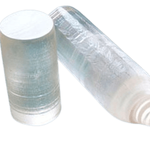
| Growth Method | Czochralski |
| Hardness | 6.5 (Mohs) |
| Melting Point | 1840℃ |
| Density | 6.74 g/cm³ |
| Thermal Expansion | 10 x 10⁻⁶/℃ |
| Permittivity | ε = 22 |
| Color and Appearance | Colorless to light brown, depending on annealing |
Specifications
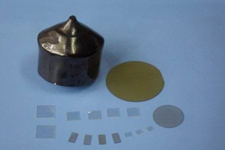
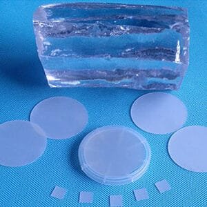
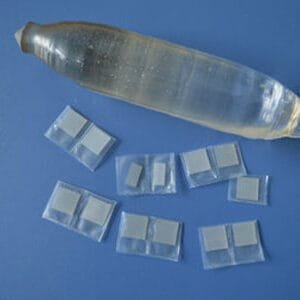
- Size: 10×3 mm, 10×5 mm, 10×10 mm, 15×15 mm, 20×20 mm, Dia 15 mm, Dia 20 mm, Dia 1”, Dia 2”
- Thickness: 0.5 mm, 1.0 mm
- Polishing: SSP or DSP
- Orientation: <100>, <110>, <111>
- Redirection Precision: ±0.5°
- Edge Redirection: 2° (special 1° available)
- Angle of Crystalline: Custom sizes and orientations available
- Surface Roughness (Ra): ≤5Å (5µm × 5µm)
Packaging Details
TFM ensures that LSAT substrates are securely packaged in class 100 clean bags or wafer containers within a class 1000 clean room to maintain product quality and cleanliness.
Explore high-performance LSAT Substrates (Lanthanum Strontium Aluminum Tantalum Oxide) from TFM for advanced thin film applications and high-temperature superconducting research.
Reviews
There are no reviews yet.