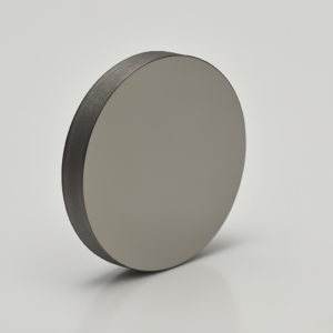
Magnesium Oxide Wafer (MgO)
Magnesium Oxide (MgO) single crystal wafers are vital components in advanced film technology applications, including magnetic, semiconductor, and optical films, as well as high-temperature superconducting films. These wafers are essential for fabricating high-temperature superconducting microwave filters and other critical devices for mobile communication equipment.
Key Physical Properties
| Property | Value |
|---|---|
| Material | MgO |
| Structure | Cubic |
| Lattice (Å) | a = 4.130 |
| Growth Method | Special Arc Melting |
| Hardness | 5.5 (Mohs) |
| Purity | 99.95% |
| Crystal Cleavage Plane | <100> |
| Melting Point | 2800℃ |
| Density | 3.58 g/cm³ |
| Thermal Expansion | 11.2 (x 10⁻⁶/℃) |
| Permittivity | ε = 9.65 |
| Optical Transmission | >90% (200 |
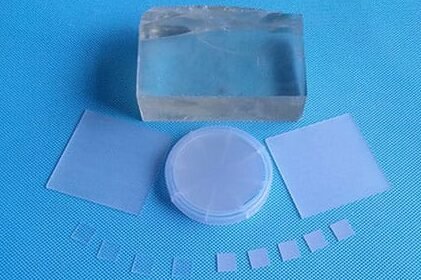
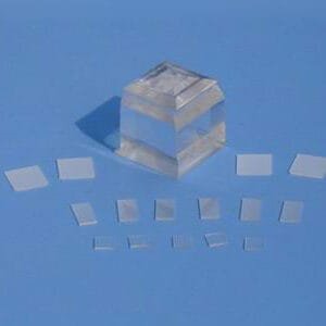
Specifications
- Size: 10×3 mm, 10×5 mm, 10×10 mm, 15×15 mm, 20×20 mm, Dia 2” x 0.33 mm, Dia 2” x 0.43 mm
- Thickness: 0.5 mm, 1.0 mm
- Polishing: SSP or DSP
- Orientation: <001>
- Redirection Precision: ±0.5°
- Edge Redirection: 2° (special 1° available)
- Angle of Crystalline: Custom sizes and orientations available
- Surface Roughness (Ra): ≤5Å (5µm × 5µm)
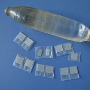
Packaging Details
TFM ensures that Magnesium Oxide wafers are securely packaged in class 100 clean bags or wafer containers within a class 1000 clean room to maintain product quality and cleanliness.
Explore superior Magnesium Oxide Wafers (MgO) from TFM, ideal for advanced film technology and high-temperature applications.
Reviews
There are no reviews yet.