
Introduction
Manganese (II) Selenide (MnSe) Sputtering Target is a chalcogenide compound material known for its semiconducting and magnetic characteristics. As part of the manganese chalcogenide family, MnSe has attracted attention in spintronic research, optoelectronic materials, and magnetic semiconductor studies. When used in sputtering systems, MnSe enables the deposition of uniform thin films with controlled stoichiometry and reproducible electronic properties.
Detailed Description
Our MnSe Sputtering Targets are produced from carefully synthesized manganese and selenium sources to ensure accurate stoichiometry and phase purity. Maintaining the correct Mn:Se ratio is critical, as slight deviations can influence carrier concentration, magnetic ordering, and optical absorption in the resulting thin films.
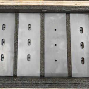
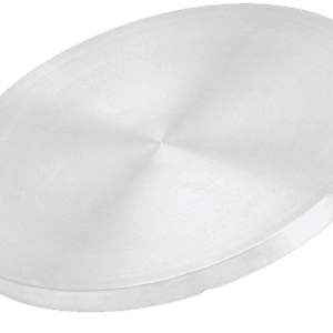
The targets are consolidated using optimized powder processing and sintering techniques to achieve high density and structural uniformity. A dense microstructure reduces particle generation and enhances plasma stability during RF sputtering. Due to its semiconducting nature, MnSe targets are typically operated under RF sputtering conditions to ensure stable deposition and consistent film composition. Custom diameters, thicknesses, and optional bonding to metallic backing plates are available to meet specific system requirements.
Applications
Manganese (II) Selenide Sputtering Targets are widely used in advanced thin film research and specialized device fabrication, including:
Magnetic semiconductor thin films
Spintronic and magneto-optical device research
Chalcogenide-based optoelectronic materials
Infrared-sensitive thin films
Functional coatings for sensing applications
Academic and industrial R&D in transition metal chalcogenides
Technical Parameters
| Parameter | Typical Value / Range | Importance |
|---|---|---|
| Chemical Composition | MnSe | Determines magnetic and semiconducting behavior |
| Purity | 99.9% – 99.99% | Minimizes impurity-induced defects |
| Diameter | 25 – 200 mm (custom available) | Compatible with sputtering systems |
| Thickness | 3 – 6 mm | Influences target lifetime |
| Density | ≥ 95% theoretical | Improves plasma stability |
| Sputtering Mode | RF sputtering | Suitable for semiconducting compounds |
| Bonding | Unbonded / Cu backing (optional) | Enhances thermal management |
Comparison with Related Materials
| Material | Key Advantage | Typical Application |
|---|---|---|
| MnSe | Magnetic semiconductor properties | Spintronic research |
| MnS | Wider band gap | Optical coatings |
| FeSe | Superconductivity research | Advanced physics studies |
| ZnSe | Transparent semiconductor | Optoelectronics |
FAQ
| Question | Answer |
|---|---|
| Can MnSe targets be customized? | Yes, size, thickness, purity, and bonding options can be tailored. |
| Is RF sputtering required? | Yes, MnSe is typically deposited using RF sputtering. |
| How is the target packaged? | Vacuum-sealed with protective cushioning and export-grade cartons or crates. |
| Is MnSe suitable for magnetic thin films? | Yes, MnSe is widely studied for magnetic semiconductor applications. |
Packaging
Our Manganese (II) Selenide Sputtering Targets are meticulously labeled and vacuum-sealed to prevent moisture exposure and contamination. Protective export-grade packaging ensures safe transport and long-term storage stability.
Conclusion
Manganese (II) Selenide (MnSe) Sputtering Target provides a reliable platform for depositing high-quality magnetic and semiconducting chalcogenide thin films. With precise composition control, high density, and customizable configurations, it is well suited for advanced spintronic, optoelectronic, and research-driven applications.
For detailed specifications and a quotation, please contact us at sales@thinfilmmaterials.com

Reviews
There are no reviews yet.