
 MSDS File
Product Overview
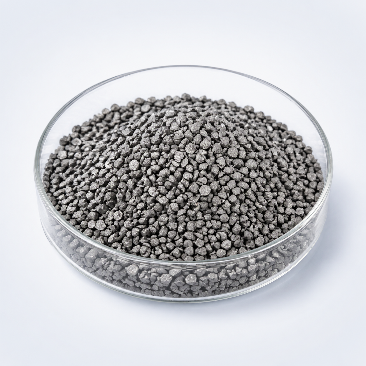
N-type Silicon Evaporation Materials (Si) is a composition-specific evaporation source for vacuum thin-film deposition and materials-development work. The correct process depends on melting point, vapor pressure, decomposition behavior, reactivity, source geometry, and the required film composition. TFM can supply custom source forms and purities according to the evaporator and application.
Explore related source materials and forms in the Evaporation Materials catalog.
Evaporation Behavior and Process Considerations
The evaporation source should be selected according to the material’s melting point, vapor pressure, decomposition behavior, and compatibility with the boat, crucible, or e-beam hearth. A gradual conditioning cycle and stable rate monitoring are useful starting practices for repeatable deposition.
Technical Data
| Parameter | Typical Value / Range | Importance |
|---|---|---|
| Material | N-type Silicon (Si) | Semiconductor functionality |
| Dopant Type | P / As / Sb (customizable) | Defines electrical properties |
| Purity | 99.999% (5N) or higher | Reduces contamination |
| Resistivity | 0.001 – 10 Ω·cm (customizable) | Controls conductivity |
| Form | Pieces / Granules / Pellets | Compatible with evaporation systems |
| Melting Point | 1414°C | Stable high-temperature behavior |
| Deposition Method | E-beam / Resistive Evaporation | Process flexibility |
| Material | Key Advantage | Typical Application |
|---|---|---|
| N-type Silicon | Electron-rich semiconductor | Conductive thin films |
| P-type Silicon | Hole-rich semiconductor | Complementary device layers |
| Intrinsic Silicon | Very high resistivity | Insulating or buffer layers |
| Amorphous Silicon | Low-temperature deposition compatibility | Solar cells |
| Question | Answer |
|---|---|
| Can dopant concentration be customized? | Yes, resistivity and dopant levels can be tailored to meet specific device requirements. |
| Is the material suitable for electron beam evaporation? | Yes, it is optimized for stable melting in e-beam systems. |
| How is oxide formation controlled? | Materials are surface-cleaned and vacuum-sealed to minimize oxidation prior to use. |
| Can small research quantities be supplied? | Yes, flexible quantities are available for R&D purposes. |
| How is it packaged? | Vacuum-sealed, moisture-protected packaging ensures clean delivery. |
Typical Thin-Film Applications
- Thin-film R&D requiring a composition-specific evaporation source
- Optical, semiconductor, electronic, energy, and advanced-material coating studies depending on the compound
- Custom PVD research using pellets, pieces, granules, or other source forms
Source Form and Ordering Considerations
For quotation, provide material, purity, source form, particle or piece size, quantity, evaporation method, and any boat, basket, crucible, or e-beam hearth constraints. If the material will be used for a specific coating stack, sharing the intended film thickness or deposition application can help with source-form selection and packaging recommendations.
Frequently Asked Questions
How should the evaporation method for N-type Silicon be selected?
Select the method from melting point, vapor pressure, decomposition behavior, charge size, and the available source hardware. Resistance heating and electron-beam evaporation are the most common starting options.
What source form is available for N-type Silicon?
Depending on the material, pellets, pieces, granules, tablets, or other compact forms can be reviewed for compatibility with the customer’s evaporator.
Why is source preconditioning important for N-type Silicon?
Gradual preheating can remove adsorbed gas, stabilize the charge, and reduce spitting or pressure excursions before film deposition.
Can the film composition differ from the N-type Silicon source?
Yes. Preferential evaporation, decomposition, re-evaporation, and substrate conditions can all change the final film composition.
Does purity matter for N-type Silicon evaporation material?
Yes. Source purity contributes directly to the contamination budget of the deposited film, together with chamber, crucible, and substrate cleanliness.
What information should I send TFM for a N-type Silicon RFQ?
Provide material or formula, purity, source form and size, quantity, evaporation method, holder constraints, and any film or documentation requirements.
Reviews
There are no reviews yet.