Introduction
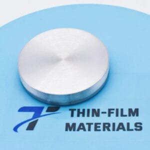
The N-type Silicon Sputtering Target (N-Doped Si) is a semiconductor-grade deposition material widely used in thin film fabrication for microelectronics, photovoltaics, and advanced electronic devices. By introducing donor impurities such as phosphorus, arsenic, or antimony into the silicon lattice, N-type silicon provides enhanced electrical conductivity through the presence of free electrons.
In Physical Vapor Deposition (PVD) processes such as DC magnetron sputtering, N-type silicon targets are used to deposit high-quality silicon-based thin films with controlled electrical properties. These films are commonly applied in semiconductor devices, solar cells, thin film transistors, and research involving silicon-based functional layers.
Detailed Description
N-type Silicon Sputtering Targets are manufactured from high-purity silicon that has been precisely doped with donor elements to achieve the desired electrical conductivity. The silicon is typically produced through processes such as zone refining, crystal growth, and controlled doping to ensure uniform impurity distribution and high material purity.
The doping process introduces atoms with additional valence electrons into the silicon crystal lattice. Common dopants include phosphorus (P), arsenic (As), or antimony (Sb). These dopants create free electrons that increase the electrical conductivity of the silicon material, allowing the sputtering target to be used effectively in conductive sputtering systems.
N-doped silicon targets are typically compatible with DC magnetron sputtering, which requires electrically conductive materials to sustain the plasma discharge. The improved conductivity provided by N-type doping ensures stable sputtering rates and uniform film deposition.
The resulting thin films retain semiconductor properties and can be used as functional layers in various electronic and photovoltaic devices. Control of dopant concentration allows precise adjustment of electrical resistivity and carrier concentration, which is critical for semiconductor manufacturing.
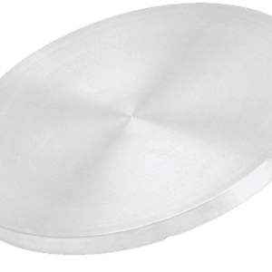
N-type silicon sputtering targets are available in circular discs, rectangular plates, and custom geometries compatible with different sputtering cathodes. For larger targets or high-power sputtering systems, the targets may be bonded to copper backing plates using indium bonding or elastomer bonding to improve heat dissipation and mechanical stability.
High-density targets help maintain stable sputtering performance, reduce particle generation, and ensure uniform thin film quality.
Applications
Thin films deposited from N-type Silicon Sputtering Targets are used in a variety of semiconductor and electronic applications:
Semiconductor device fabrication – conductive silicon layers used in integrated circuits.
Thin film transistors (TFTs) – active semiconductor layers in display technologies.
Photovoltaic devices – silicon layers used in solar cells.
Microelectromechanical systems (MEMS) – silicon films used in microfabricated devices.
Optoelectronic components – semiconductor layers used in optical sensors and photodetectors.
Research and development – semiconductor thin film studies in academic and industrial laboratories.
Technical Parameters
| Parameter | Typical Value / Range | Importance |
|---|---|---|
| Purity | 99.999% (5N) typical | High purity ensures semiconductor-grade film quality |
| Dopant Type | P / As / Sb | Determines electrical conductivity |
| Resistivity | Custom range (e.g., 0.001–10 Ω·cm) | Controls carrier concentration |
| Diameter | 25 – 300 mm (custom) | Compatible with various sputtering systems |
| Thickness | 3 – 10 mm | Influences sputtering rate and target lifetime |
| Bonding | Copper backing plate (optional) | Improves heat transfer and structural stability |
Comparison with Related Materials
| Material | Key Advantage | Typical Application |
|---|---|---|
| N-type Silicon (N-doped Si) | High electron conductivity | Semiconductor devices and photovoltaic layers |
| P-type Silicon | Hole conductivity | Complementary semiconductor structures |
| Undoped Silicon | High purity but low conductivity | Research and insulating layers |
FAQ
| Question | Answer |
|---|---|
| What does N-type silicon mean? | N-type silicon contains donor dopants such as phosphorus or arsenic that introduce extra electrons, increasing electrical conductivity. |
| Why is doping required for sputtering targets? | Doping improves electrical conductivity, allowing the target to be used in DC magnetron sputtering systems. |
| Can the resistivity be customized? | Yes, dopant concentration can be adjusted to achieve specific resistivity levels required by semiconductor processes. |
| Are bonded targets available? | Yes, N-type silicon targets can be bonded to copper backing plates for improved thermal management during sputtering. |
| Which industries use N-type silicon sputtering targets? | Semiconductor manufacturing, solar cell production, display technologies, and advanced electronics research laboratories. |
Packaging
Our N-type Silicon Sputtering Targets are meticulously tagged and labeled externally to ensure efficient identification and maintain strict quality control standards. Each target is vacuum-sealed and carefully packaged with protective cushioning materials to prevent contamination or mechanical damage during storage and transportation. Export-grade cartons or wooden crates are used to ensure safe international delivery.
Conclusion
The N-type Silicon Sputtering Target (N-Doped Si) is an essential semiconductor material used for depositing conductive silicon thin films in microelectronics, photovoltaic devices, and advanced electronic systems. Controlled doping allows precise tuning of electrical properties while maintaining high material purity and deposition stability.
With customizable dopant concentrations, high-purity silicon, and precision manufacturing, N-type silicon sputtering targets provide reliable performance for both semiconductor production and research applications.
For detailed specifications and a quotation, please contact us at sales@thinfilmmaterials.com.


Reviews
There are no reviews yet.