
 MSDS File
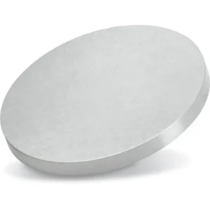
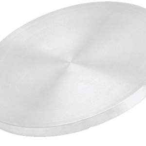
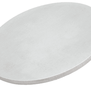
N-type Silicon Sputtering Target Description
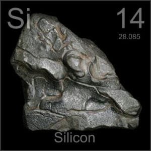 The N-type silicon sputtering target is dark gray with a bluish tinge. Silicon, symbolized as “Si,” derives its name from the Latin word ‘silex’ or ‘silicis,’ meaning flint. It was first mentioned in 1824 and discovered by J. Berzelius, who also accomplished its isolation. Silicon has an atomic number of 14 and is located in Period 3, Group 14 of the periodic table, within the p-block. Its relative atomic mass is 28.0855 Daltons, with the number in brackets indicating the measurement uncertainty.
N-type Silicon Sputtering Target Specification
| Material Type | N-type Silicon |
| Symbol | Si |
| Color/Appearance | Dark Gray with a Bluish Tinge, Semi-Metallic |
| Melting Point | 1,410 °C |
| Density | 2.32 g/cc |
| Thermal Conductivity | 150 W·m-1·K-1 (25°C) |
| Thermal Expansion | 2.6 x 10⁻⁶/K (25°C) |
| Available Sizes | Dia.: 1.0″, 2.0″, 3.0″, 4.0″, 5.0″, 6.0″ Thick: 0.125″, 0.250″ |
We also offer other customized shapes and sizes of the sputtering targets; please Contact Us for more information.
N-type Silicon Sputtering Target Bonding Services
Specialized bonding services for N-type Silicon Sputtering Targets, including indium and elastomeric bonding techniques, enhance performance and durability. Thin Film Materials (TFM) ensures high-quality solutions that meet industry standards and customer needs.
We also offer custom machining of backing plates, which is essential for sputtering target assembly. This comprehensive approach improves target design flexibility and performance in thin film deposition. Our channels provide detailed information about bonding materials, methods, and services, helping clients make informed decisions.

N-type Silicon Sputtering Target Application
Applications of N-Type Silicon Sputtering Target
The N-type silicon sputtering target is used in various applications, including:
- Thin film deposition
- Decoration
- Semiconductor manufacturing
- Displays
- LED and photovoltaic devices
- Functional coatings
- Optical information storage
- Glass coating for automotive and architectural glass
- Optical communications
Other Applications of Silicon
- Solar Cells: Silicon is a key material in the production of solar cells.
- Transistors: Widely used in the manufacturing of transistors.
- Semiconductors: Essential in semiconductor devices.
- Rectifiers and Solid-State Devices: Used extensively in electronics and space sectors for rectifiers and other solid-state devices.
N-type Silicon Sputtering Target Packaging
Our N-type silicon sputter coater targets are clearly tagged and labeled externally to ensure efficient identification and quality control. We take great care to prevent any damage during storage and transportation, ensuring the targets remain in pristine condition.
Get Contact
TFM offers N-type Silicon Sputtering Targets in various forms, purities, sizes, and prices. We specialize in high-purity thin film deposition materials with optimal density and minimal grain sizes, which are ideal for semiconductor, CVD, and PVD applications in display and optics. Contact Us for current pricing on sputtering targets and other deposition materials that are not listed.
Reviews
There are no reviews yet.