Introduction
Nb-Doped SrTiO₃ Substrate (Niobium-Doped Strontium Titanate) is a conductive perovskite oxide single crystal widely used in advanced thin film research and oxide electronics. By introducing controlled niobium doping into the SrTiO₃ lattice, the substrate transitions from an insulating material to a stable n-type conductor while maintaining excellent crystallographic quality.
This unique combination of structural compatibility and electrical conductivity makes Nb-Doped SrTiO₃ Substrate a preferred platform for epitaxial growth of complex oxide films, superconducting materials, ferroelectrics, and functional heterostructures.
Detailed Description
Nb-Doped SrTiO₃ Substrate is engineered by substituting Ti⁴⁺ sites with Nb⁵⁺ ions within the perovskite lattice. This substitution introduces free carriers, enabling controlled conductivity without significantly altering lattice parameters. As a result, it retains the excellent lattice match properties of SrTiO₃ while providing a conductive base layer for thin film deposition.
Key features include:
Precisely controlled Nb doping levels (commonly 0.05–0.7 wt% or customized mol%)
Low resistivity suitable for bottom electrode applications
Atomically flat surface finish (single-side or double-side polished)
High crystalline quality with low dislocation density
Stable thermal performance for high-temperature deposition processes
Surface preparation is critical for oxide epitaxy. Substrates are typically chemo-mechanically polished to achieve step-terrace structures after annealing, supporting high-quality epitaxial growth via PLD, MBE, sputtering, or CVD techniques.
The conductive nature of Nb-Doped SrTiO₃ Substrate eliminates the need for additional bottom electrode layers in many experiments, reducing interface complexity and improving measurement accuracy in electrical characterization.
Applications
Nb-Doped SrTiO₃ Substrate is widely applied in research institutions, semiconductor labs, and advanced materials development:
Oxide electronics and heterostructures
Superconducting thin film deposition
Ferroelectric and multiferroic materials research
Resistive switching (ReRAM) devices
Transparent conducting oxide (TCO) studies
Spintronic materials development
Photocatalytic and energy-related oxide films
Sensor and MEMS-related oxide integration
Its conductive behavior makes it especially valuable when electrical transport measurements are required directly through the substrate.
Technical Parameters
| Parameter | Typical Value / Range | Importance |
|---|---|---|
| Crystal Structure | Perovskite (Cubic) | Enables epitaxial oxide growth |
| Nb Doping Level | 0.05 – 0.7 wt% (customizable) | Controls conductivity |
| Resistivity | 0.001 – 0.1 Ω·cm | Suitable for bottom electrode use |
| Orientation | (100), (110), (111) | Determines film growth mode |
| Surface Finish | SSP / DSP | Influences film quality |
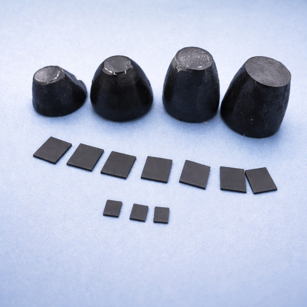
| Size | 5×5 mm – 20×20 mm (custom) | Matches deposition holders |
| Thickness | 0.5 mm – 1.0 mm | Mechanical stability & thermal resistance |
Comparison with Related Materials
| Material | Key Advantage | Typical Application |
|---|---|---|
| Nb-Doped SrTiO₃ Substrate | Conductive & lattice-matched oxide base | Oxide electronics & superconductors |
| Undoped SrTiO₃ | High insulation | Dielectric studies |
| LaAlO₃ | Better lattice match for specific films | High-mobility interfaces |
| Sapphire (Al₂O₃) | Excellent thermal stability | General oxide deposition |
Compared with undoped SrTiO₃, the niobium-doped variant significantly simplifies device structures that require electrical measurement through the substrate. Compared with sapphire, it offers superior lattice compatibility for perovskite oxide films.
FAQ
| Question | Answer |
|---|---|
| Can the doping concentration be customized? | Yes, Nb content can be adjusted to meet specific resistivity requirements. |
| Is the substrate suitable for high-temperature deposition? | Yes, it maintains structural stability in typical oxide deposition temperatures above 800°C. |
| What orientations are available? | Standard orientations include (100), (110), and (111); others can be discussed upon request. |
| Can you provide atomically flat surfaces? | Yes, substrates can be supplied with epi-ready surface preparation. |
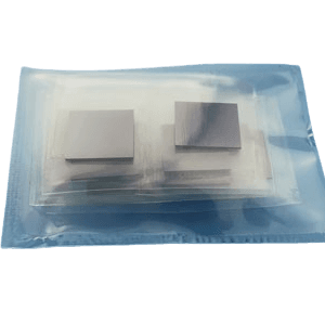
| How are substrates packaged? | Individually packed in cleanroom-grade vacuum-sealed containers to prevent contamination. |
Packaging
Our Nb-Doped SrTiO₃ Substrate products are meticulously tagged and labeled externally to ensure efficient identification and maintain high standards of quality control. We take great care to prevent any potential damage during storage and transportation, ensuring the substrates arrive in perfect condition.
Conclusion
Nb-Doped SrTiO₃ Substrate provides an ideal combination of structural compatibility, electrical conductivity, and thermal stability for advanced oxide thin film research and device fabrication. Its tunable doping levels and high crystalline quality make it a reliable choice for laboratories and industrial R&D environments worldwide.
For detailed specifications and a quotation, please contact us at sales@thinfilmmaterials.com.

Reviews
There are no reviews yet.