 MSDS File
Introduction
Nickel(II) Oxide Evaporation Materials (NiO) are high-purity oxide sources designed for vacuum deposition of p-type semiconducting and functional thin films. As a wide bandgap transition metal oxide, NiO is widely used in optoelectronics, resistive switching devices, electrochromic systems, and transparent electronics research.
In physical vapor deposition (PVD) processes, NiO evaporation materials enable controlled formation of uniform oxide films with tunable electrical and optical properties. Proper stoichiometry and purity are essential to achieving consistent film conductivity and stability.
Detailed Description
Nickel(II) Oxide (NiO) is a stable cubic oxide with a melting point above 1900°C and a bandgap typically in the range of 3.6–4.0 eV. Due to its insulating or semiconducting nature depending on defect structure, NiO films are commonly used in electronic and optoelectronic devices.
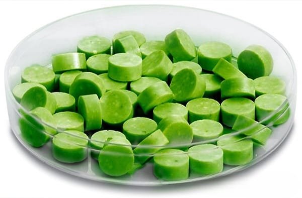
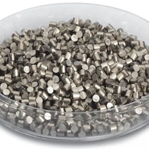
Evaporation materials are generally supplied in:
Sintered pellets
Granules
Pressed tablets
Custom-cut ceramic pieces
Manufacturing emphasizes:
High phase purity to avoid metallic Ni contamination
Controlled oxygen stoichiometry
Dense microstructure (≥95% theoretical density)
Uniform grain size for stable evaporation
NiO evaporation materials are typically used in electron beam evaporation or high-temperature thermal evaporation systems. Reactive oxygen control during deposition can be applied to fine-tune film stoichiometry and electrical characteristics.
NiO thin films commonly exhibit:
P-type semiconducting behavior
High optical transparency in visible range
Good chemical stability
Compatibility with perovskite and oxide-based systems
These properties make NiO attractive for hole transport layers and functional oxide stacks.
Applications
Nickel(II) Oxide Evaporation Materials are widely used in:
Transparent p-type semiconductor films
Electrochromic devices
Resistive switching memory (ReRAM) research
Perovskite solar cell hole transport layers
Gas sensors and catalytic thin films
Spintronic and oxide electronics research
Thin film capacitors and dielectric studies
NiO is frequently integrated into multilayer structures where controlled conductivity and transparency are required.
Technical Parameters
| Parameter | Typical Value / Range | Importance |
|---|---|---|
| Chemical Formula | NiO | Defines oxide semiconductor properties |
| Purity | 99.9% – 99.99% | Reduces defects & improves film quality |
| Form | Pellets / Granules / Pieces | Compatible with evaporation sources |
| Density | ≥ 95% theoretical | Enhances deposition stability |
| Bandgap | ~3.6–4.0 eV | Influences optical transparency |
| Deposition Method | E-beam / Thermal (with O₂ control) | Maintains stoichiometry |
Custom pellet sizes and material forms can be provided according to specific vacuum system requirements.
Comparison with Related Oxide Materials
| Material | Key Advantage | Typical Application |
|---|---|---|
| NiO | Stable p-type oxide semiconductor | Transparent electronics |
| ZnO | N-type transparent oxide | Transparent conductive films |
| TiO₂ | High dielectric & photocatalytic activity | Optical coatings |
| Cu₂O | P-type semiconductor | Photovoltaic research |
Compared to ZnO, NiO provides p-type conductivity, making it complementary in transparent electronic and heterojunction applications.
FAQ
| Question | Answer |
|---|---|
| Is oxygen control required during deposition? | Oxygen control may be used to optimize film stoichiometry and conductivity. |
| Is NiO suitable for thermal evaporation? | Yes, but electron beam evaporation is often preferred for better control. |
| Can custom pellet sizes be supplied? | Yes, size and form can be tailored to match your equipment. |
| Is NiO compatible with perovskite solar cells? | Yes, it is widely used as a hole transport layer in perovskite devices. |
| Are certifications available? | Yes, chemical analysis and batch traceability documents can be provided. |
Packaging
Our Nickel(II) Oxide Evaporation Materials are meticulously tagged and labeled externally to ensure efficient identification and maintain high standards of quality control. Materials are carefully vacuum-sealed or packed in moisture-resistant containers to maintain integrity during storage and transportation.
Conclusion
Nickel(II) Oxide Evaporation Materials (NiO) provide a reliable solution for p-type semiconductor films and functional oxide thin film applications. With controlled purity, stable evaporation performance, and customizable configurations, they support advanced research and industrial deposition processes.
For detailed specifications and a quotation, please contact us at sales@thinfilmmaterials.com.


Reviews
There are no reviews yet.